Session 6: Synthesis & Physical Design
Homework
- Synthesize your design — review gate count and check for unintended latches
- Run place and route flow
- Analyze timing reports — identify and fix any violations
- Generate GDS and review layout in KLayout
Design Synthesis
Now to work on the synthesis of the RTL I wrote and simulated. Basically the synthesis converts the verilog RTL to gate-level netlist made of standard cells.
Verilog RTL to logic synthesis to Gate-level netlist.
I ran the yosys command and was able to get following output:
> yosys
yosys> read_verilog digital_password_lock.v debounce.v

1. Executing Verilog-2005 frontend: digital_password_lock.v
Parsing Verilog input from `digital_password_lock.v' to AST representation.
Generating RTLIL representation for module `\password_core'.
Generating RTLIL representation for module `\register4'.
Generating RTLIL representation for module `\digital_password_lock'.
Successfully finished Verilog frontend.

2. Executing Verilog-2005 frontend: debounce.v
Parsing Verilog input from `debounce.v' to AST representation.
Generating RTLIL representation for module `\debounce'.
Successfully finished Verilog frontend.
Yosys sucessfully loaded my files and all the modules were recognized.
Next was to run the hierarchy :
yosys> hierarchy -check -top digital_password_lock

3. Executing HIERARCHY pass (managing design hierarchy).

3.1. Analyzing design hierarchy..
Top module:  \digital_password_lock
Used module:     \password_core
Used module:     \register4
Used module:     \debounce
Parameter \CLK_FREQ = 50000000

3.2. Executing AST frontend in derive mode using pre-parsed AST for module `\debounce'.
Parameter \CLK_FREQ = 50000000
Generating RTLIL representation for module `$paramod\debounce\CLK_FREQ=s32'00000010111110101111000010000000'.

3.3. Analyzing design hierarchy..
Top module:  \digital_password_lock
Used module:     \password_core
Used module:     \register4
Used module:     $paramod\debounce\CLK_FREQ=s32'00000010111110101111000010000000

3.4. Analyzing design hierarchy..
Top module:  \digital_password_lock
Used module:     \password_core
Used module:     \register4
Used module:     $paramod\debounce\CLK_FREQ=s32'00000010111110101111000010000000
Removing unused module `\debounce'.
Removed 1 unused modules.
Hierarchy step worked as well.
Next I ran the following inside yosys:
synth -top digital_password_lock stat check
yosys> stat

5. Printing statistics.

=== $paramod\debounce\CLK_FREQ=s32'00000010111110101111000010000000 ===

        +----------Local Count, excluding submodules.
        |
      118 wires
      154 wire bits
        8 public wires
       26 public wire bits
        4 ports
        4 port bits
      151 cells
       40   $_ANDNOT_
        4   $_AND_
        1   $_DFFE_PN0P_
       22   $_DFF_PN0_
       15   $_NAND_
        5   $_NOR_
        1   $_NOT_
       13   $_ORNOT_
       31   $_OR_
        6   $_XNOR_
       13   $_XOR_

=== digital_password_lock ===

        +----------Local Count, excluding submodules.
        |
       62 wires
      145 wire bits
       15 public wires
       51 public wire bits
        7 ports
       12 port bits
       79 cells
       18   $_ANDNOT_
        3   $_AND_
        5   $_DFFE_PN0P_
       12   $_DFF_PN0_
        1   $_MUX_
        7   $_NAND_
        2   $_NOR_
        3   $_NOT_
        5   $_ORNOT_
       12   $_OR_
        2   $_XNOR_
        9   $_XOR_
        3 submodules
        1   $paramod\debounce\CLK_FREQ=s32'00000010111110101111000010000000
        1   password_core
        1   register4

=== password_core ===

        +----------Local Count, excluding submodules.
        |
        4 wires
        7 wire bits
        2 public wires
        5 public wire bits
        2 ports
        5 port bits
        3 cells
        1   $_ANDNOT_
        1   $_AND_
        1   $_ORNOT_

=== register4 ===

        +----------Local Count, excluding submodules.
        |
        5 wires
       11 wire bits
        5 public wires
       11 public wire bits
        5 ports
       11 port bits
        4 cells
        4   $_DFFE_PN0P_

=== design hierarchy ===

        +----------Count including submodules.
        |
      237 digital_password_lock
      151 $paramod\debounce\CLK_FREQ=s32'00000010111110101111000010000000
        3 password_core
        4 register4

        +----------Count including submodules.
        |
      189 wires
      317 wire bits
       30 public wires
       93 public wire bits
       18 ports
       32 port bits
        - memories
        - memory bits
        - processes
      237 cells
       59   $_ANDNOT_
        8   $_AND_
       10   $_DFFE_PN0P_
       34   $_DFF_PN0_
        1   $_MUX_
       22   $_NAND_
        7   $_NOR_
        4   $_NOT_
       19   $_ORNOT_
       43   $_OR_
        8   $_XNOR_
       22   $_XOR_
        3 submodules
        1   $paramod\debounce\CLK_FREQ=s32'00000010111110101111000010000000
        1   password_core
        1   register4
The design was synthesized in Yosys using digital_password_lock as the top module. The synthesis stat showed a total of 237 cells in the full design hierarchy. This includes 44 flip-flop cells and a combination of logic gates such as AND, OR, NAND, NOR, XOR, and XNOR. A significant portion of the cell count comes from the debounce module, which contains internal counters and sequential logic. The synthesized design therefore includes both combinational and sequential hardware as expected.
Next I ran the check command
yosys> check
6. Executing CHECK pass (checking for obvious problems).
Checking module $paramod\debounce\CLK_FREQ=s32'00000010111110101111000010000000...
Checking module digital_password_lock...
Checking module password_core...
Checking module register4...
Found and reported 0 problems.
Through this since no problems was detected, no intented latches were inferred during synthesis.
Then I mapped it it to sky130 cells, I used the command from the class page, I forgot about the path and it gave me some error. So I made sure to give the correct path:
dfflibmap -liberty /foss/pdks/sky130A/libs.ref/sky130_fd_sc_hd/lib/sky130_fd_sc_hd__tt_025C_1v80.lib
abc -liberty /foss/pdks/sky130A/libs.ref/sky130_fd_sc_hd/lib/sky130_fd_sc_hd__tt_025C_1v80.lib
I also generated the gate-level netlist after cleaning it up
yosys> clean
Removed 0 unused cells and 254 unused wires.

yosys> write_verilog -noattr synth.v

7. Executing Verilog backend.

7.1. Executing BMUXMAP pass.

7.2. Executing DEMUXMAP pass.
Dumping module `$paramod\debounce\CLK_FREQ=s32'00000010111110101111000010000000'.
Dumping module `\digital_password_lock'.
Dumping module `\password_core'.
Dumping module `\register4'.
Place and Route
For the P&R step, I have to expect the following: - Floorplanning - Power planning - Cell placement - Clock tree synthesis - Routing - Fill
With this I ran the openroad command in my project folder.
I ran the following command:
read_lef $::env(PDK_ROOT)/sky130A/libs.ref/sky130_fd_sc_hd/lef/sky130_fd_sc_hd.lef
read_liberty $::env(PDK_ROOT)/sky130A/libs.ref/sky130_fd_sc_hd/lib/sky130_fd_sc_hd__tt_025C_1v80.lib

There were a long list of warning, however at the end since the library was created, I moved on to the next step.
Read Synthesized Netlist For the constraints file I used the one provided in the lib, but made a few changes as per my projects requirement :
read_verilog synth.v //generated in yosys
link_design
read_sdc constraints.sdc
initialize_floorplan -utilization 50 -aspect_ratio 1 -core_space 2
However I got the follofilewing error as I tried initializing the floorplan. The floorplan basically defines the chip shape and usable core area. It also decides how much space the design gets and where cells are allowed to live.
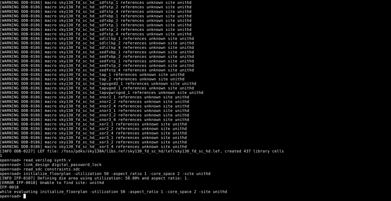
I realized the best and the fastest step would be to review other student's documentation. I looked into Þórarinn's documentaion and saw he faced a smilar issue. I followed his steps and that fixed my issue.
set design_name digital_password_lock
set top_module  digital_password_lock
set netlist     "synth.v"
set sdc_file    "constraints.sdc"

set out_dir "openroad_out"
file mkdir $out_dir

set pdk_root $::env(PDK_ROOT)
Through his explanation, I was able to understand that set is used for creating variable and setting value to it.
With this step, I started from the technology setup again and then read the synth file and linked my design, which gave no output and then the constraints file was read, which also gave no output.

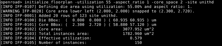
Finally initialized the floor plan, which gave the following output. This time there was no error and everything worked out.
Now onto next step, I looked into the openflow documentation. As per the documentation, once the floorplan is initialized , next step is to place the I/O pins.
The make_tracks sets up the routing tracks for each metal layer.
make_tracks
place_pins -hor_layers met3 -ver_layers met2
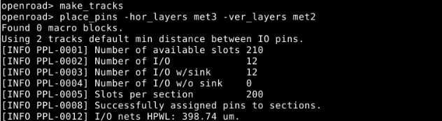
12 I/O pins were found and placed sucessfully.
With this the next step was to insert tapcell, according to the documentation tap cells connect the substrate to VDD or ground which prevents body from floating. I ran the following command:
tapcell -tapcell_master sky130_fd_sc_hd__tapvpwrvgnd_1

Next step was to create a power distribution network, I used the command from the class page:
source $::env(PDK_ROOT)/sky130A/libs.tech/openlane/sky130_fd_sc_hd/tracks.info

After getting this error I looked into the power distribution network and instead of the tracks.info file, we need to source a pdn.tcl. I looked into how it is supposed to look and saw in this github page how to organize the script, which I used.
#global connections
add_global_connection -net {VDD} -inst_pattern {.*} -pin_pattern {^VDD$} -power
add_global_connection -net {VDD} -inst_pattern {.*} -pin_pattern {^VDDPE$}
add_global_connection -net {VDD} -inst_pattern {.*} -pin_pattern {^VDDCE$}
add_global_connection -net {VDD} -inst_pattern {.*} -pin_pattern {VPWR}
add_global_connection -net {VDD} -inst_pattern {.*} -pin_pattern {VPB}

add_global_connection -net {VSS} -inst_pattern {.*} -pin_pattern {^VSS$} -ground
add_global_connection -net {VSS} -inst_pattern {.*} -pin_pattern {^VSSE$}
add_global_connection -net {VSS} -inst_pattern {.*} -pin_pattern {VGND}
add_global_connection -net {VSS} -inst_pattern {.*} -pin_pattern {VNB}

global_connect

# voltage domain
set_voltage_domain -name {CORE} -power {VDD} -ground {VSS}

# standard cell grid
define_pdn_grid -name {grid} -voltage_domains {CORE} -pins {met4}

add_pdn_stripe -grid {grid} -layer {met1} -width {0.48} -pitch {5.44} -offset {0} -followpins
add_pdn_stripe -grid {grid} -layer {met4} -width {0.8} -pitch {40} -offset {10}

add_pdn_connect -grid {grid} -layers {met1 met4}
With this I ran the command:
source ./pdn.tcl
pdngen

Next was the global placement and I ran the following command. This stage is where we get to see a rough placement but they are not legalized yet.
global_placement -density 0.80
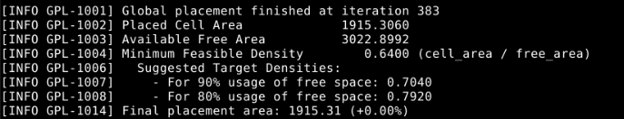
Then the detailed placement,this is cleanup stage where It places cells onto valid rows/sites, removes overlaps, and makes the placement physically legal for later clock tree synthesis and routing.
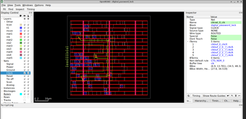
Next step was to do the clock tree synthesis. CTS is the stage where the tool builds the clock path for the whole design.:
clock_tree_synthesis
[WARNING CTS-0104] Clock wire resistance/capacitance values are zero.
Use set_wire_rc to set them.
[INFO CTS-0050] Root buffer is sky130_fd_sc_hd__clkbuf_2.
[INFO CTS-0051] Sink buffer is sky130_fd_sc_hd__clkbuf_4.
[INFO CTS-0052] The following clock buffers will be used for CTS:
                    sky130_fd_sc_hd__clkbuf_2
                    sky130_fd_sc_hd__clkbuf_4
[INFO CTS-0049] Characterization buffer is sky130_fd_sc_hd__clkbuf_4.
[INFO CTS-0007] Net "clk" found for clock "clk".
[INFO CTS-0010]  Clock net "clk" has 44 sinks.
[INFO CTS-0008] TritonCTS found 1 clock nets.
[INFO CTS-0097] Characterization used 2 buffer(s) types.
[INFO CTS-0201] 0 blockages from hard placement blockages and placed macros will be used.
[INFO CTS-0027] Generating H-Tree topology for net clk.
[INFO CTS-0028]  Total number of sinks: 44.
[INFO CTS-0030]  Number of static layers: 0.
[INFO CTS-0020]  Wire segment unit: 13600  dbu (13 um).
[INFO CTS-0023]  Original sink region: [(3945, 14900), (49485, 52980)].
[INFO CTS-0024]  Normalized sink region: [(0.290074, 1.09559), (3.6386, 3.89559)].
[INFO CTS-0025]     Width:  3.3485.
[INFO CTS-0026]     Height: 2.8000.
 Level 1
    Direction: Horizontal
    Sinks per sub-region: 22
    Sub-region size: 1.6743 X 2.8000
[INFO CTS-0034]     Segment length (rounded): 1.
 Level 2
    Direction: Vertical
    Sinks per sub-region: 11
    Sub-region size: 1.6743 X 1.4000
[INFO CTS-0034]     Segment length (rounded): 1.
[INFO CTS-0032]  Stop criterion found. Max number of sinks is 15.
[INFO CTS-0035]  Number of sinks covered: 44.
[INFO CTS-0018]     Created 5 clock buffers.
[INFO CTS-0012]     Minimum number of buffers in the clock path: 2.
[INFO CTS-0013]     Maximum number of buffers in the clock path: 2.
[INFO CTS-0015]     Created 5 clock nets.
[INFO CTS-0016]     Fanout distribution for the current clock = 9:2, 11:1, 15:1..
[INFO CTS-0017]     Max level of the clock tree: 2.
[INFO CTS-0098] Clock net "clk"
[INFO CTS-0099]  Sinks 47
[INFO CTS-0100]  Leaf buffers 0
[INFO CTS-0101]  Average sink wire length 65.45 um
[INFO CTS-0102]  Path depth 2 - 2
[INFO CTS-0207]  Dummy loads inserted 3
Next was to run the global and detailed route and I got a lot of error. With this I re-did the entire process, because I had a doubt my floor plan might be the issue.
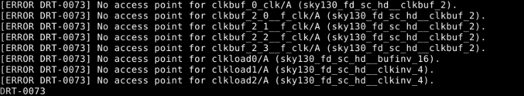
I redid everything but I ended up getting the same error. I checked online and I found someone had a similar error OpenRoad. I tried the following command as suggested, which is run before detailed_route and run in the GUI:
detailed_route_debug -pa -pa_markers -pin _3504_:A1
After looking into the open road documents:
For the pin access failure, I tried adding placement padding, restricting the CTS buffer list, and disabling dummy loads.
set_placement_padding \
  -masters {sky130_fd_sc_hd__clkbuf_4 sky130_fd_sc_hd__clkbuf_8 sky130_fd_sc_hd__clkbuf_16 sky130_fd_sc_hd__clkinv_2} \
  -left 1 -right 1

set_cts_config -buf_list {sky130_fd_sc_hd__clkbuf_4 sky130_fd_sc_hd__clkbuf_8 sky130_fd_sc_hd__clkbuf_16}

clock_tree_synthesis -dont_use_dummy_load
detailed_placement
pin_access -verbose 2
I looked into the pdn and started making changes on it. I tested in different cases: -- No PDN and No CTS works - PDN and No CTS works - No PDN, CTS fails - PDN, CTS fails Which made me conclude that CTS was causing the issue.
However I did make changes in the PDN file, I simplified it:
#Global connections
add_global_connection -net {VDD} -inst_pattern {.*} -pin_pattern {^VDD$}   -power
add_global_connection -net {VDD} -inst_pattern {.*} -pin_pattern {^VDDPE$}
add_global_connection -net {VDD} -inst_pattern {.*} -pin_pattern {^VDDCE$}
add_global_connection -net {VDD} -inst_pattern {.*} -pin_pattern {^VPWR$}
add_global_connection -net {VDD} -inst_pattern {.*} -pin_pattern {^VPB$}

add_global_connection -net {VSS} -inst_pattern {.*} -pin_pattern {^VSS$}   -ground
add_global_connection -net {VSS} -inst_pattern {.*} -pin_pattern {^VSSE$}
add_global_connection -net {VSS} -inst_pattern {.*} -pin_pattern {^VGND$}
add_global_connection -net {VSS} -inst_pattern {.*} -pin_pattern {^VNB$}

global_connect

set_voltage_domain -name {CORE} -power {VDD} -ground {VSS}

#PDN grid
define_pdn_grid -name stdcell_grid -voltage_domains {CORE} -pins {met5}
add_pdn_stripe -grid stdcell_grid -layer met1 -followpins
add_pdn_stripe -grid stdcell_grid -layer met4 -width 1.0 -pitch 100 -offset 20
add_pdn_stripe -grid stdcell_grid -layer met5 -width 1.0 -pitch 100 -offset 20
add_pdn_connect -grid stdcell_grid -layers {met1 met4}
add_pdn_connect -grid stdcell_grid -layers {met4 met5}
I also made changes on the floorplan and placement. Also fixed the CTS configuration and finally I re-run the placement after CTS.
This is how my final run.tcl file looked:
set design_name digital_password_lock
set top_module digital_password_lock
set netlist "synth.v"
set sdc_file "constraints.sdc"
set pdk_root $::env(PDK_ROOT)
read_lef $pdk_root/sky130A/libs.ref/sky130_fd_sc_hd/techlef/sky130_fd_sc_hd__nom.tlef
read_lef $pdk_root/sky130A/libs.ref/sky130_fd_sc_hd/lef/sky130_fd_sc_hd.lef
read_liberty $pdk_root/sky130A/libs.ref/sky130_fd_sc_hd/lib/sky130_fd_sc_hd__tt_025C_1v80.lib
read_verilog $netlist
link_design $top_module
read_sdc $sdc_file
initialize_floorplan -utilization 20 -aspect_ratio 1 -core_space 25 -site unithd
make_tracks
place_pins -hor_layers met3 -ver_layers met2
tapcell -distance 14 -tapcell_master sky130_fd_sc_hd__tapvpwrvgnd_1
# source pdn.tcl
#pdngen
global_placement -density 0.30 -routability_driven
detailed_placement
set_wire_rc -signal -layer met2
set_wire_rc -clock -layer met3
set_cts_config -buf_list {sky130_fd_sc_hd__clkbuf_2}
clock_tree_synthesis
detailed_placement
pin_access -verbose 2
global_route
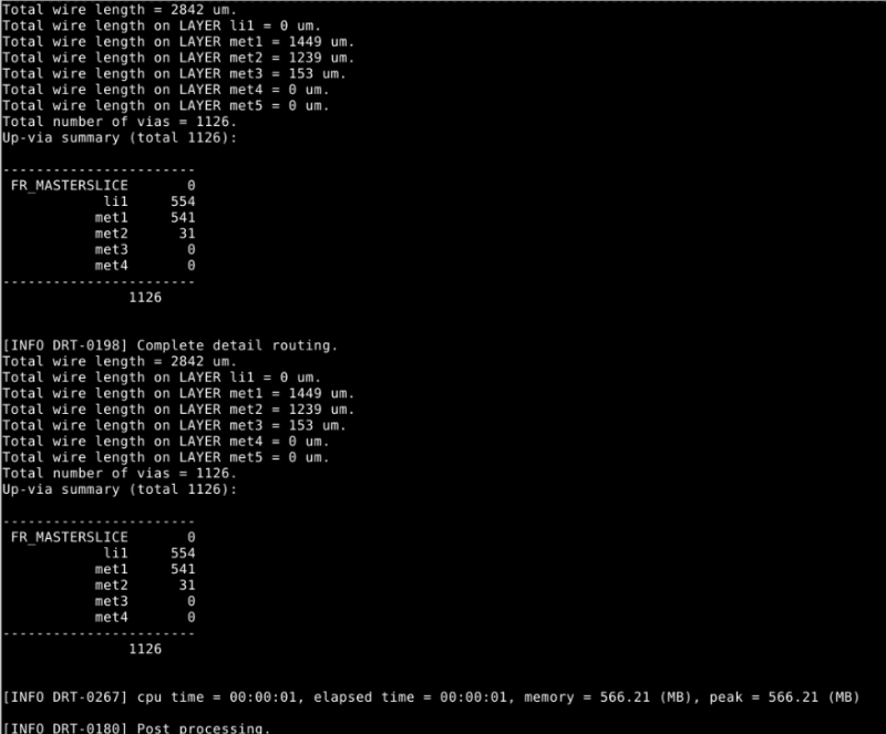
detailed_route
report_checks
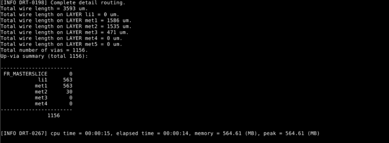
Finally my detailed routing worked and I got my post-route timing report as well.
Timing reports
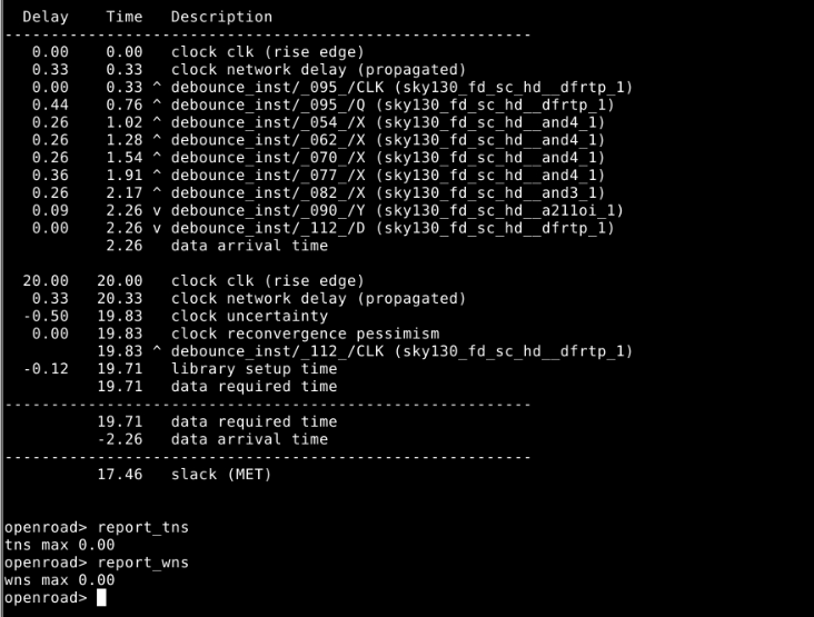
report_checks
report_wns
report_tns
Power Analysis
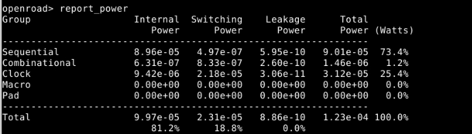
report_power
The total power consumption of the design is approximately 0.123 mW. Most of the power is due to internal power (81.2%), followed by switching power (18.8%), while leakage power is negligible. Most of the power is consumed by sequential elements (73.4%) and the clock network (25.4%), which is expected since clock signals toggle frequently and drive flip-flops.The low total power reflects the small size of the design and moderate switching activity.
Generate GDS and review layout
After the outputs were written using the following command:
write_def
write_verilog
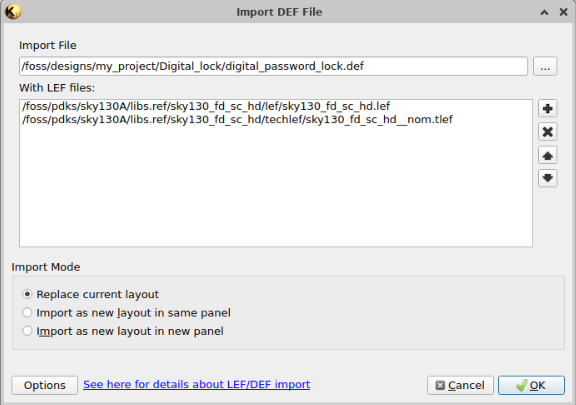
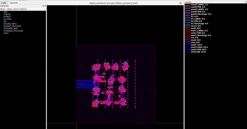
I looked into KLayout documentation to see how I can import def file and get gds.
I pressed on the import the def/lef file, then loaded my def and lef file along with the .lef lib files.
Once that was done, I was able to view the following layout as such:
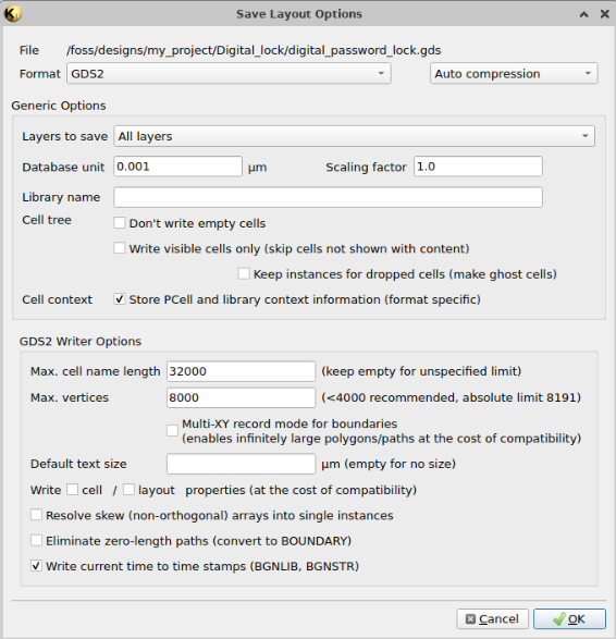
Now to export the def to gds file, I did save as and got the following:
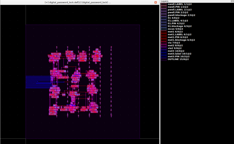
Which then, when I opened in Klayout looked like this:
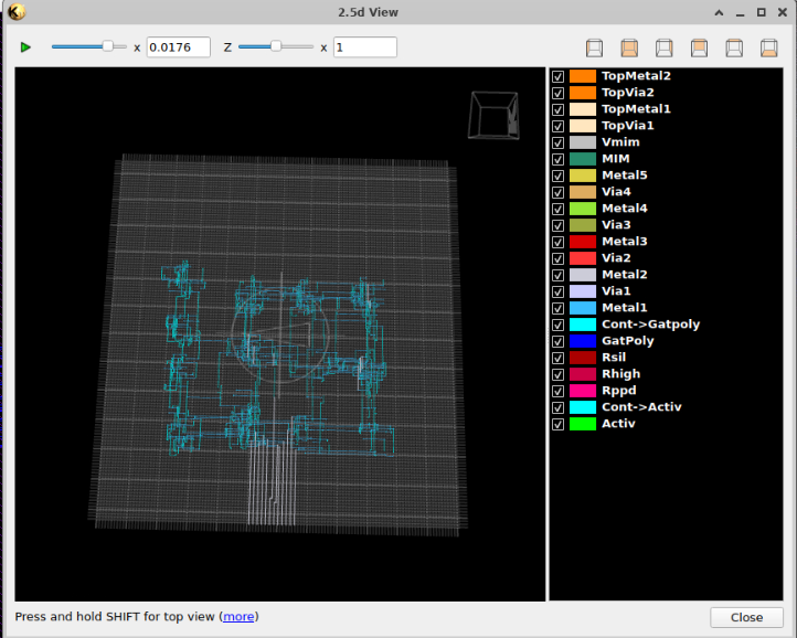
I also tried the 2.5d viewer for fun: