Session 7: Packaging & Board Design
- Run final DRC/LVS on your design (done in the final project)
- Document your chip: functionality, pin assignments, and interface details (e.g., timing parameters, frequencies, baud rates)
- Develop a verification test plan
- Prepare your presentation for Thursday!
Sessions closure
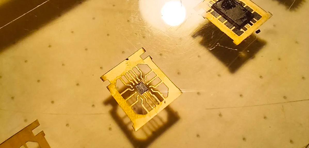
The last session was primarily spent working on the final project. I spent a lot of time with my up/down ALU unit, so I wanted to bring that to a proper closure by making a well-deserved old-school DIP-14 package for it.
This project was the first RTL-to-GDS flow I completed, so it will always have a special place in memory.
I named it balu 9000, short for basic ALU.
Chip functionality
The design receives a clock and reset signal and performs a simple up/down operation depending on the control inputs.
The behavior is controlled by:
OPC0andOPC1which define the operationUP_ENandDOWN_ENwhich enable counting directionRX_RDYwhich acts as a simple handshake input
When an operation completes the result is emitted through the TX output and a TX_VALID signal indicates that the output is ready.
The goal of this chip was not performance but to build my own complete minimal ASIC pipeline, going from:
Operating data
Since balu 9000 is an experimental ASIC prototype, the following operating parameters are based on simulation and the synthesis results.
| Parameter | Value | Notes |
|---|---|---|
| Supply voltage | 1.8 V | Sky130 core voltage |
| Clock frequency | ~10–50 MHz | Conservative estimate based on simple logic depth |
| Reset | Active low (RSTN) |
Must be asserted during startup |
| Logic interface | CMOS | Standard digital inputs |
| Output interface | CMOS | Direct digital output |
Package
        ┌──────────────────┐
  VDD  ─┤ 1             14 ├─ VSS
 OPC0  ─┤ 2             13 ├─ TX_VAL
 OPC1  ─┤ 3             12 ├─ TX
 RSTN  ─┤ 4    balu     11 ├─ DOWN_EN
TX_RDY ─┤ 5    9000     10 ├─ UP_EN
  VPB  ─┤ 6              9 ├─ CLK
  VSS  ─┤ 7              8 ├─ VNB
        └──────────────────┘
pinout
| Pin | Signal | Direction | Notes |
|---|---|---|---|
| 1 | VDD | Power | Core supply |
| 2 | OPC0 | Input | Opcode bit 0 |
| 3 | OPC1 | Input | Opcode bit 1 |
| 4 | RSTN | Input | Active-low reset |
| 5 | TX_RDY | Input | Input ready / handshake |
| 6 | VPB | Power | Bulk bias, tie to VDD |
| 7 | VSS | Ground | Ground |
| 8 | VNB | Ground | Bulk ground, tie to VSS |
| 9 | CLK | Input | System clock |
| 10 | UP_EN | Input | Count up enable |
| 11 | DOWN_EN | Input | Count down enable |
| 12 | TX | Output | Output data |
| 13 | TX_VAL | Output | Output valid flag |
| 14 | VSS | Ground | Ground |
Wirebond diagram
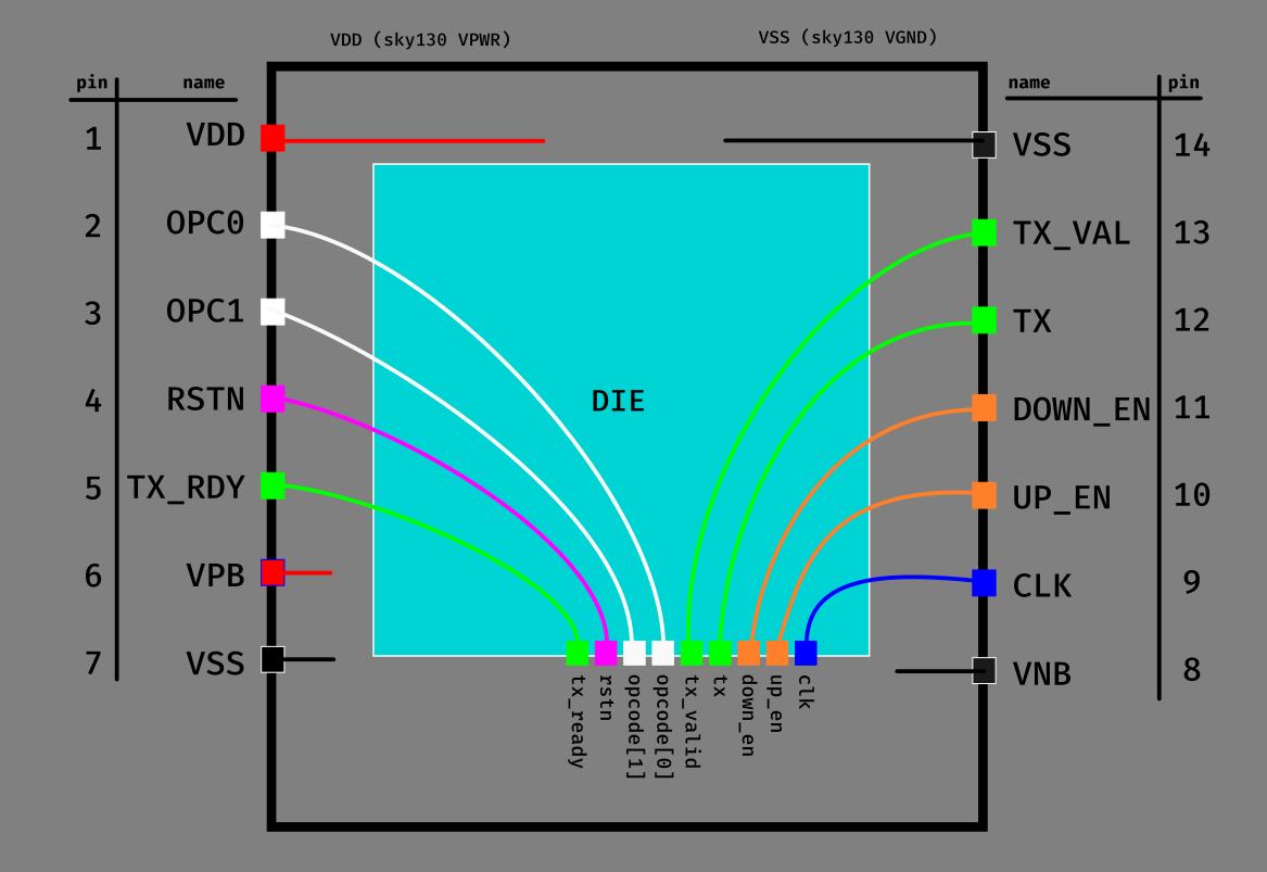
Figure 1 - Conceptual wire-bond diagram of the
balu 9000ASIC in a DIP-14 package. Pin ordering follows the pad order on the die to minimize bond wire crossings.
Verification test plan
The design was verified primarily through RTL simulation before running the physical design flow.
Verification steps included:
- Clock generation A testbench clock was generated to drive the design.
- Reset behavior The reset signal was toggled to confirm the design returns to a known state.
- Opcode testing Different opcode combinations were applied to confirm the ALU selects the correct operation.
- Enable control
UP_ENandDOWN_ENwere toggled to verify correct counting direction. - Output validation
TX_VALIDwas monitored to ensure that output data is flagged correctly.
Waveforms were inspected using Surfer waveform viewer during the simulation phase.