Skip to content

UV Laser - PCB Settings

This work was done by Svavar Konráðsson check out more of his work here

EasyTrace 5000

I've found that if I go into the folder with the Gerber files, take the F_Cu.gbr file into Ricardo's EasyTrace 5000 and use the Filled Polygon option in Isolation Routing, the process takes only half as long as when you use the PNG of the traces and ablate all the copper with the laser.

I first select Start with Laser:

laser

Then Select UV:

laser

Then I drag the F_Cu.gbr file into Isolation Routing:

laser

On the right, I select SVG and xTool Studio:

laser

Then on the left, I select the F_Cu.gbr file:

laser

Now I get the offset settings on the right side, for this board a 1mm offset worked well. I use the Filled Polygon option.

laser

Then I hit Generate Laser Paths and export the SVG.

I import the SVG into xTool Studio.

xTool studio settings

I use Gerber2PNG to get the PNG files and import them into the same project in the xTool Studio software. Then I use the Align function to align them all together and then I use the Trace function in xTool studio to turn them into vectors.

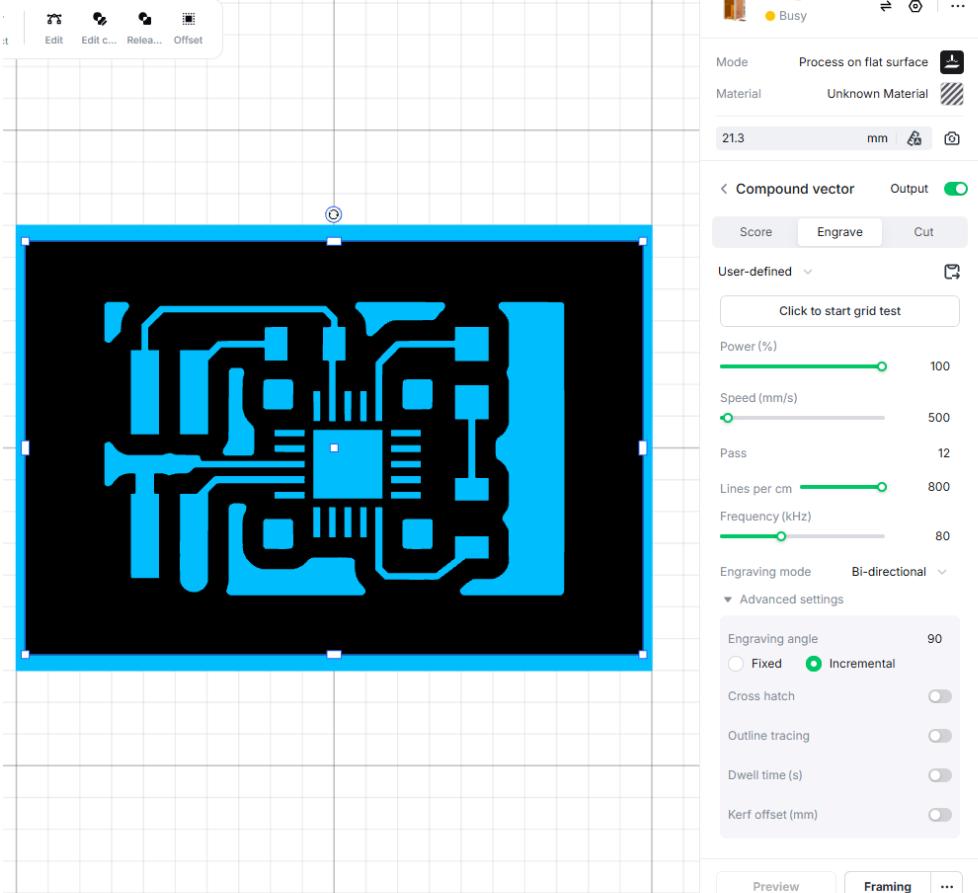
Here are the settings I used for the traces:

laser

Here are the settings I used for the holes and outline:

laser

I make the different operations different colors and then arrange the order of operations by arranging the layers on the left.

Then I need to select the three dots next to the black Process. Under Processing path (which means order of operations) I select User defining. Then I check By layer:

laser

Good UV Settings - xTool .xcs file

Outcome

laser

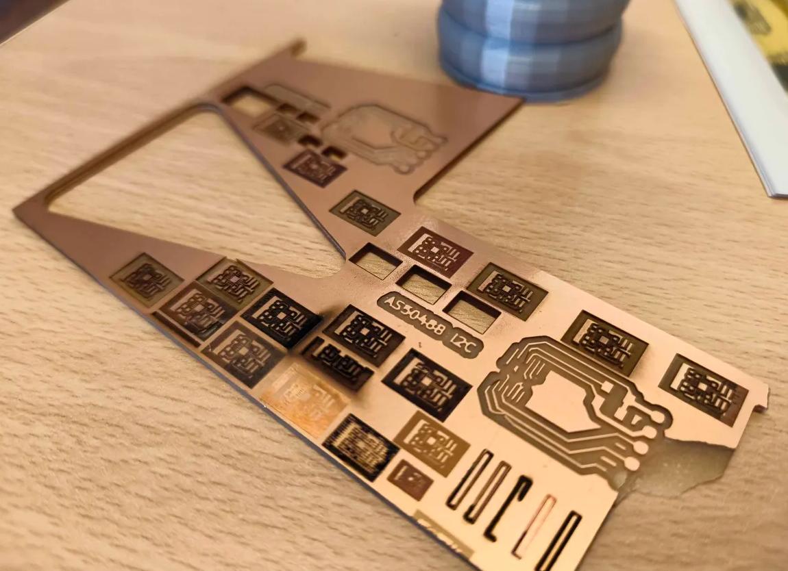
I've found that the flatness of the PCB stock matters a lot. When it curves, I get inconsistent results, like this:

laser

This was after 8 passes. After 2 more passes, all the copper was cleared:

laser

There may be a little bit of debris/oxidation/charring on the traces after laser processing. I think they would work fine, but to make the traces a bit nicer I used a wet sanding sponge to clean them up:

laser

After sanding the board looks like this:

laser

The reason for using the UV laser on this board was the fine spaces between the pads for the power-only USB-C connector in the top right corner. I enlarged the pads that the metal housing goes into a lot, to get a better mechanical connection. I tore up the connector on the last USB-C board I made.

Here is the final result:

laser