Session 07: Packaging & Board Design
The topic of this final sessionn is the last stage to release my IC design to be physical product. Also, we need to prepare for the final presentation…
Homework
- Run final DRC/LVS on your design
- Document your chip: functionality, pin assignments, and interface details (e.g., timing parameters, frequencies, baud rates)
- Develop a verification test plan
- Prepare your presentation for Thursday!
Assignment 1: Run final DRC/LVS on your design
First, I tried to open magic to check drc. But, There are couple of problems to install magic in current MacOS.
I downloaded source code here and tried to install,,, but when doing make command, the following result come out…
yosuke@ysk-M1Pro magic % make
--- making header file database/database.h
./scripts/makedbh ./database/database.h.in database/database.h
Version: ImageMagick 7.1.2-16 Q16-HDRI aarch64 23761 https://imagemagick.org
Copyright: (C) 1999 ImageMagick Studio LLC
License: https://imagemagick.org/license/
Features: Cipher DPC HDRI Modules
Delegates (built-in): bzlib freetype heic jng jpeg lcms ltdl lzma png tiff webp xml zlib zstd
Compiler: clang (17.0.0)
Usage: import [options ...] [ file ]

Image Settings:
  -adjoin              join images into a single multi-image file
  -border              include window border in the output image
  -channel type        apply option to select image channels

.....

By default, 'file' is written in the MIFF image format.  To
specify a particular image format, precede the filename with an image
format name and a colon (i.e. ps:image) or specify the image type as
the filename suffix (i.e. image.ps).  Specify 'file' as '-' for
standard input or output.
import: delegate library support not built-in '' (X11) @ error/import.c/ImportImageCommand/1302.
./scripts/makedbh: line 9: syntax error near unexpected token `('
./scripts/makedbh: line 9: `database_h_in = open(sys.argv[1], encoding="utf8").read()'
make: *** [database/database.h] Error 2
yosuke@ysk-M1Pro magic %
It seems “ImageMagick“‘s help command is loaded.... very strange.... I think recent ImageMagick (after 7.0) changed the image convert command from “convert” to “magick”.... Is it affected…? I don’t know well…
So, I tried to install from macport.
sudo port install magic
I could installed by using macport.
But next, I tried to start magic with the following command.
magic -T ~/.ciel/sky130A/libs.tech/magic/sky130A.tech run_drc.tcl
But, the magic is crashed. Because this command tried to start magic with GUI, but there are some troubles when running X11 on macos....
So, I found to start magic without GUI interface as follow.
magic -dnull -noconsole -T ~/.ciel/sky130A/libs.tech/magic/sky130A.tech

Magic 8.3 revision 508 - Compiled on Tue Sep 23 19:47:06 UTC 2025.
Starting magic under Tcl interpreter
Using the terminal as the console.
Using NULL graphics device.
Input style sky130(): scaleFactor=2, multiplier=2
The following types are not handled by extraction and will be treated as non-electrical types:
    ubm
Processing system .magicrc file
Using technology "sky130A", version 1.0.575-2-g7b70722
%
Then, I could start it.
I wrote the following command list for DRC check of my IC design.
lef read ~/.ciel/sky130A/libs.ref/sky130_fd_sc_hd/techlef/sky130_fd_sc_hd__nom.tlef
lef read ~/.ciel/sky130A/libs.ref/sky130_fd_sc_hd/lef/sky130_fd_sc_hd.lef
def read adder_subtractor.def
load top_wrapper
select top cell
drc check
drc catchup
set count [drc count total]
puts "DRC_ERRORS: $count"
quit
Then, run again magic with reading these commands
magic -dnull -noconsole -T ~/.ciel/sky130A/libs.tech/magic/sky130A.tech run_drc.tcl
The result is here:
Magic 8.3 revision 508 - Compiled on Tue Sep 23 19:47:06 UTC 2025.
Starting magic under Tcl interpreter
Using the terminal as the console.
Using NULL graphics device.
Input style sky130(): scaleFactor=2, multiplier=2
The following types are not handled by extraction and will be treated as non-electrical types:
    ubm
Processing system .magicrc file
Loading "run_drc.tcl" from command line.
Reading LEF data from file /Users/yosuke/.ciel/sky130A/libs.ref/sky130_fd_sc_hd/techlef/sky130_fd_sc_hd__nom.tlef.
This action cannot be undone.
LEF read, Line 82 (Message): Unknown keyword "ANTENNAMODEL" in LEF file; ignoring.
LEF read, Line 83 (Message): Unknown keyword "ANTENNADIFFSIDEAREARATIO" in LEF file; ignoring.
LEF read, Line 116 (Message): Unknown keyword "MINENCLOSEDAREA" in LEF file; ignoring.
LEF read, Line 118 (Message): Unknown keyword "ANTENNAMODEL" in LEF file; ignoring.
LEF read, Line 119 (Message): Unknown keyword "ANTENNADIFFSIDEAREARATIO" in LEF file; ignoring.
LEF read, Line 125 (Message): Unknown keyword "MAXIMUMDENSITY" in LEF file; ignoring.
LEF read, Line 126 (Message): Unknown keyword "DENSITYCHECKWINDOW" in LEF file; ignoring.
LEF read, Line 127 (Message): Unknown keyword "DENSITYCHECKSTEP" in LEF file; ignoring.
LEF read, Line 160 (Message): Unknown keyword "MINENCLOSEDAREA" in LEF file; ignoring.
LEF read, Line 168 (Message): Unknown keyword "ANTENNAMODEL" in LEF file; ignoring.
LEF read, Line 169 (Message): Unknown keyword "ANTENNADIFFSIDEAREARATIO" in LEF file; ignoring.
LEF read, Line 171 (Message): Unknown keyword "MAXIMUMDENSITY" in LEF file; ignoring.
LEF read, Line 172 (Message): Unknown keyword "DENSITYCHECKWINDOW" in LEF file; ignoring.
LEF read, Line 173 (Message): Unknown keyword "DENSITYCHECKSTEP" in LEF file; ignoring.
LEF read, Line 210 (Message): Unknown keyword "ANTENNAMODEL" in LEF file; ignoring.
LEF read, Line 211 (Message): Unknown keyword "ANTENNADIFFSIDEAREARATIO" in LEF file; ignoring.
LEF read, Line 213 (Message): Unknown keyword "MAXIMUMDENSITY" in LEF file; ignoring.
LEF read, Line 214 (Message): Unknown keyword "DENSITYCHECKWINDOW" in LEF file; ignoring.
LEF read, Line 215 (Message): Unknown keyword "DENSITYCHECKSTEP" in LEF file; ignoring.
LEF read, Line 252 (Message): Unknown keyword "ANTENNAMODEL" in LEF file; ignoring.
LEF read, Line 253 (Message): Unknown keyword "ANTENNADIFFSIDEAREARATIO" in LEF file; ignoring.
LEF read, Line 255 (Message): Unknown keyword "MAXIMUMDENSITY" in LEF file; ignoring.
LEF read, Line 256 (Message): Unknown keyword "DENSITYCHECKWINDOW" in LEF file; ignoring.
LEF read, Line 257 (Message): Unknown keyword "DENSITYCHECKSTEP" in LEF file; ignoring.
LEF read, Line 294 (Message): Unknown keyword "ANTENNAMODEL" in LEF file; ignoring.
LEF read, Line 295 (Message): Unknown keyword "ANTENNADIFFSIDEAREARATIO" in LEF file; ignoring.
LEF read: Processed 801 lines.
Reading LEF data from file /Users/yosuke/.ciel/sky130A/libs.ref/sky130_fd_sc_hd/lef/sky130_fd_sc_hd.lef.
This action cannot be undone.
LEF read: Processed 56536 lines.
Reading DEF data from file adder_subtractor.def.
This action cannot be undone.
  Processed 8 vias total.
  Processed 80 subcell instances total.
  Processed 19 pins total.
  Processed 2 special nets total.
  Processed 64 nets total.
DEF read: Processed 1273 lines.
DEF Read: encountered 14 warnings total.
Loading DRC CIF style.
Total DRC errors found: 836
DRC_ERRORS:
It seems a couple of errors occur.... but, it could be caused by some warning and trouble when reading lef/tech file of SKY130A pdks....
In fact, when I run the drc check in openroad, I could get the following result that represents no error. So, at this point, I believe there are no trouble for my design....
Assignment 2: Document my chip
My Chip: 4 adder/subtractor with memory register
Here is presentation slide of my IC Chip design
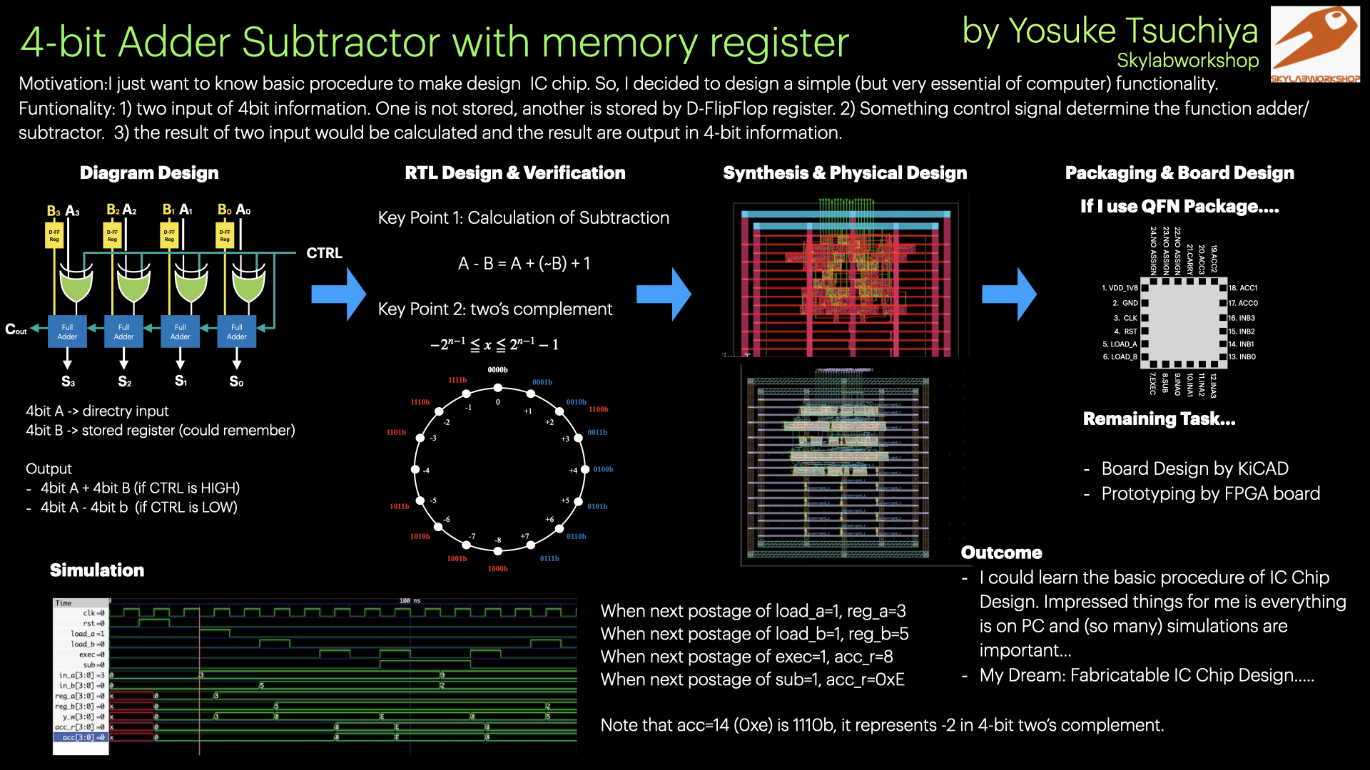
functionality
1) two input of 4bit information. And both 4bit input are stored into each register based on D-Flip-Flop. 2) Control signal determine the function adder/subtractor. When SUB = 0, addition is operated. When SUB=1, subtaction is operated. EXEC signal control the timing for those calculating operation. 3) the result of two input would be calculated and stored into Accumlation register. Then, result are output in 4-bit information.
Pin Assign
It would packaged with QFN package…
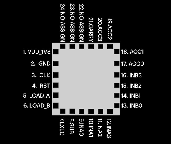
Pin assing description here.
| pin no. | pin name | direction | description |
|---|---|---|---|
| 1 | VDD_1V8 | Power | 1.8 V power supply for the chip core. |
| 2 | GND | Power | Ground reference |
| 3 | CLK | Input | System clock input. All register updates occur on the rising edge of this clock. |
| 4 | RST | Input | Synchronous reset input. Clears internal registers (reg_a, reg_b, acc) to zero when asserted. |
| 5 | LOAD_A | Input | Loads the external input INA[3:0] into register A on the next rising clock edge. |
| 6 | LOAD_B | Input | Loads the external input INB[3:0] into register B on the next rising clock edge. |
| 7 | EXEC | Input | Executes the selected arithmetic operation on the next rising clock edge and stores the result into the accumulator register. |
| 8 | SUB | Input | Operaton select. 0= addition, 1= subtraction |
| 9 | INA0 | Input | Bit 0 of 4-bit operand A external input |
| 10 | INA1 | Input | Bit 1 of 4-bit operand A external input |
| 11 | INA2 | Input | Bit 2 of 4-bit operand A external input |
| 12 | INA3 | Input | Bit 3 of 4-bit operand A external input |
| 13 | INB0 | Input | Bit 0 of 4-bit operand B external input |
| 14 | INB1 | Input | Bit 1 of 4-bit operand B external input |
| 15 | INB2 | Input | Bit 2 of 4-bit operand B external input |
| 16 | INB3 | Input | Bit 3 of 4-bit operand B external input |
| 17 | ACC0 | Output | Bit 0 of 4-bit accumulator output |
| 18 | ACC1 | Output | Bit 1 of 4-bit accumulator output |
| 19 | ACC2 | Output | Bit 2 of 4-bit accumulator output |
| 20 | ACC3 | Output | Bit 3 of 4-bit accumulator output |
| 21 | CARRY | Output | Carry output for addition, or no-borrow flag for subtraction. |
| 22 | NC | - | No connection |
| 23 | NC | - | No connection |
| 24 | NC | - | No connection |
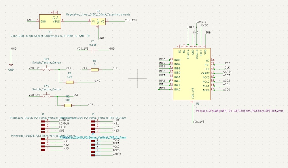
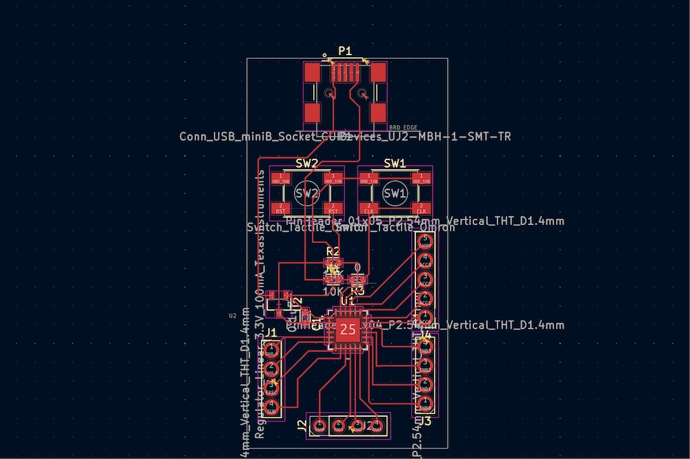
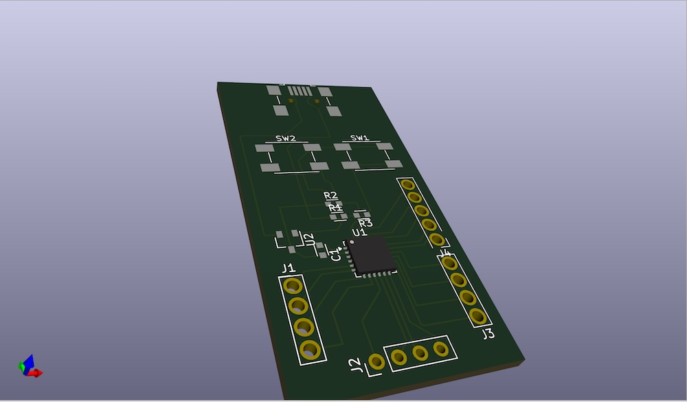
Design Evaluation Board by KiCAD
I tried to design Evaluation board of my chip with KiCAD.
Here is the schema of the eval board.
And this is the PCB design of the eval board.
Then, 3D view would be come out.
Assignment 3: Develop a verification test plan
test by simulation
I have already made a testbench as following. And, I have confirmed that works as intented.
// tb_top.sv
`timescale 1ns/1ps

module tb_top;
    logic       clk;
    logic       rst;
    logic       load_a, load_b, exec, sub;
    logic [3:0] in_a, in_b;
    wire  [3:0] acc;
    wire        carry_out;

    top_wrapper dut (
        .clk(clk),
        .rst(rst),
        .load_a(load_a),
        .load_b(load_b),
        .exec(exec),
        .sub(sub),
        .in_a(in_a),
        .in_b(in_b),
        .acc(acc),
        .carry_out(carry_out)
    );

    // 10ns period clock
    initial clk = 1'b0;
    always #5 clk = ~clk;

    initial begin
        $dumpfile("tb_top.vcd");
        $dumpvars(0, tb_top);

        // initialize
        rst    = 1'b0;
        load_a = 1'b0;
        load_b = 1'b0;
        exec   = 1'b0;
        sub    = 1'b0;
        in_a   = 4'h0;
        in_b   = 4'h0;

        // ---- reset ----
        @(negedge clk);
        rst = 1'b1;
        @(posedge clk);   // In this posedge works reset.
        @(negedge clk);
        rst = 1'b0;

        // ---- load A=3  ----
        @(negedge clk);
        in_a   = 4'd3;
        load_a = 1'b1;
        @(posedge clk);   // In this posedge, reg_a <= 3
        @(negedge clk);
        load_a = 1'b0;
        $display("[%0t] load_a done", $time);

        // ---- load B=5 ----
        @(negedge clk);
        in_b   = 4'd5;
        load_b = 1'b1;
        @(posedge clk);   // In this posedge, reg_b <= 5
        @(negedge clk);
        load_b = 1'b0;
        $display("[%0t] load_b done", $time);

        // ---- ADD: 3 + 5 = 8 ----
        @(negedge clk);
        sub  = 1'b0;
        exec = 1'b1;
        @(posedge clk);   // In this posedge, acc <= 8
        @(negedge clk);
        exec = 1'b0;
        @(posedge clk);   // wait 1 clock for displaying
        $display("[%0t] ADD 3+5 => acc=%0d (0x%0h), carry=%0b", $time, acc, acc, carry_out);

        // ---- SUB: 3 - 5 = -2 = 0xE ----
        @(negedge clk);
        sub  = 1'b1;
        exec = 1'b1;
        @(posedge clk);   // In this postage acc <= 0xE
        @(negedge clk);
        exec = 1'b0;
        @(posedge clk);
        $display("[%0t] SUB 3-5 => acc=%0d (0x%0h), carry(no-borrow)=%0b", $time, acc, acc, carry_out);

        // ---- Change external input (not loaded ----
        @(negedge clk);
        in_a = 4'd9;
        in_b = 4'd2;

        // reg_a/reg_b is still 3,5, so acc is still 8
        @(negedge clk);
        sub  = 1'b0;
        exec = 1'b1;
        @(posedge clk);
        @(negedge clk);
        exec = 1'b0;
        @(posedge clk);
        $display("[%0t] HOLD-CHECK => acc=%0d (0x%0h) (expected 8)", $time, acc, acc);

        // ---- Only update B: 3 + 2 = 5 ----
        @(negedge clk);
        load_b = 1'b1;
        @(posedge clk);   // In this posedge, reg_b <= 2
        @(negedge clk);
        load_b = 1'b0;
        $display("[%0t] load_b(2) done", $time);

        @(negedge clk);
        exec = 1'b1;
        @(posedge clk);   // In this posedge, acc <= 5
        @(negedge clk);
        exec = 1'b0;
        @(posedge clk);
        $display("[%0t] ADD 3+2 => acc=%0d (0x%0h)", $time, acc, acc);

        repeat (2) @(posedge clk);
        $finish;
    end
endmodule
Then, run the following commands, and got the result.
(base) yosuke@ysk-M1Pro design % iverilog -g2012 -o sim_addr-subtract.vvp tb_top.sv alu_core.v top_wrapper.v
(base) yosuke@ysk-M1Pro design % vvp sim_addr-subtract.vvp
VCD info: dumpfile tb_top.vcd opened for output.
[40000] load_a done
[60000] load_b done
[85000] ADD 3+5 => acc=8 (0x8), carry=0
[105000] SUB 3-5 => acc=14 (0xe), carry(no-borrow)=0
[135000] HOLD-CHECK => acc=8 (0x8) (expected 8)
[150000] load_b(2) done
[175000] ADD 3+2 => acc=5 (0x5)
tb_top.sv:118: $finish called at 195000 (1ps)
Finally, show the waveform.
gtkwave tb_top.vcd
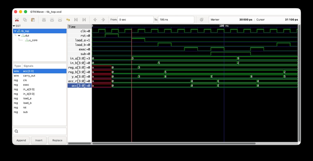
- When next postage of load_a=1, reg_a=3
- When next postage of load_b=1, reg_b=5
- When next postage of exec=1, acc_r=8
- When next postage of sub=1, acc_r=0xE
Note that acc=14 (0xe) is 1110b, it represents -2 in 4-bit two’s complement.
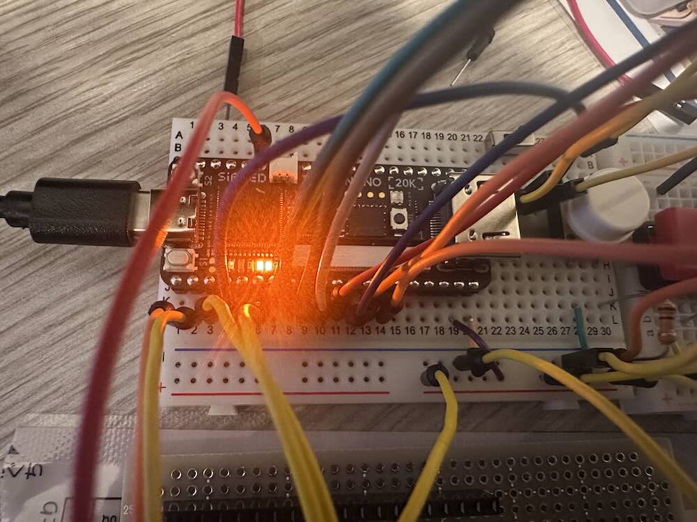
Test by Prototyping (FPGA)
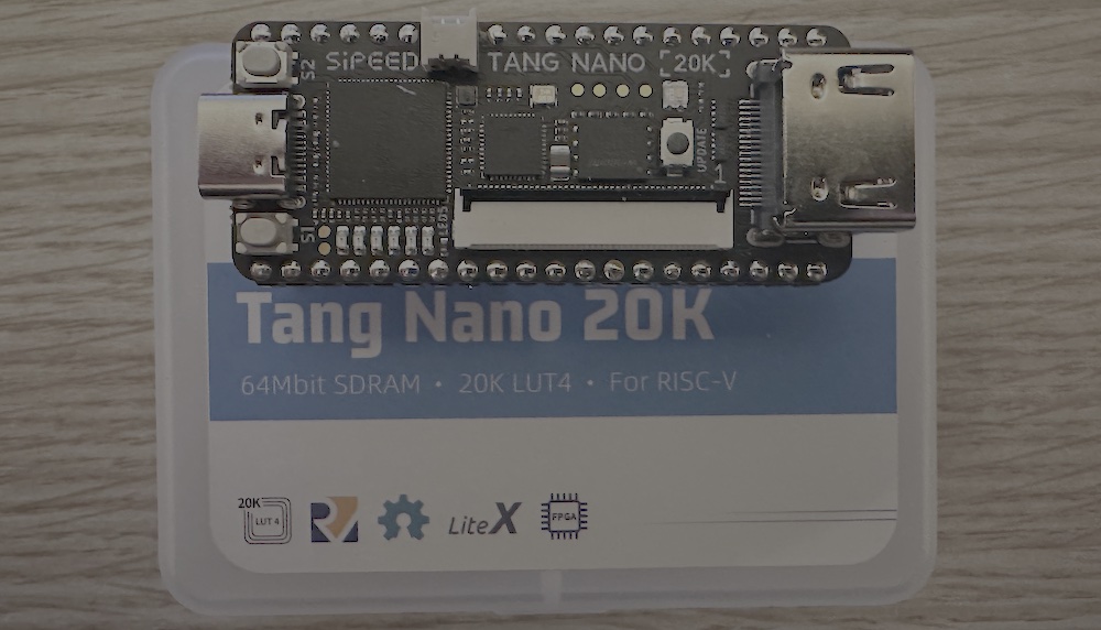
I got a FPGA board, Tang Nano 20K (Rico recommended), to prototype my chip. Here is the result of prototyping.
First, I downloaded GoWin IDE for designing and programming on this FPGA board.
- GoWin Homepage
- You need to make an account for downloading
- Also, needed to laicense registration for using it
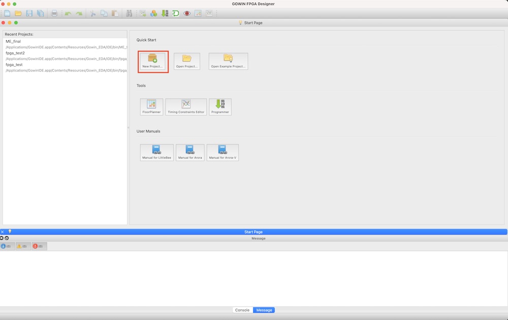
Then, start GoWin IDE and make a project.
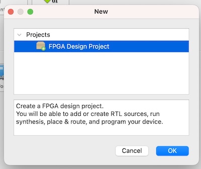
Click “New Project”.
Choose FPGA Project
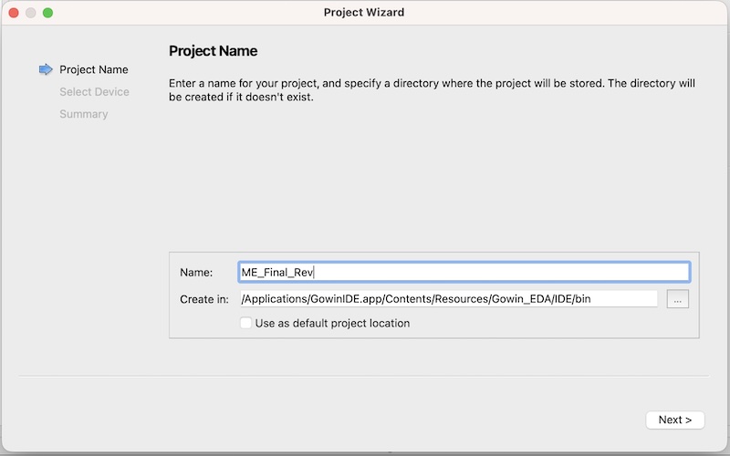
Put a project name
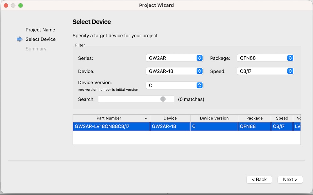
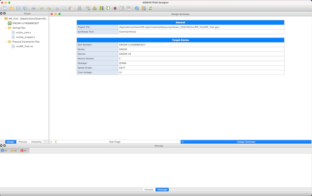
Here is the important part for configuring to write/flash program into FPGA Board and interact it. For Tang Nano 20K, I set the following.
- Series: GW2AR
- Device: GW2AR-18
- Device Version: C
- Package: QFN88
- Speed: C8/17
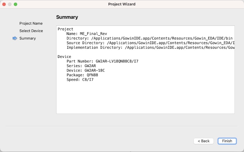
Then, finish the project setting.
Here is the main interface of GoWin IDE.
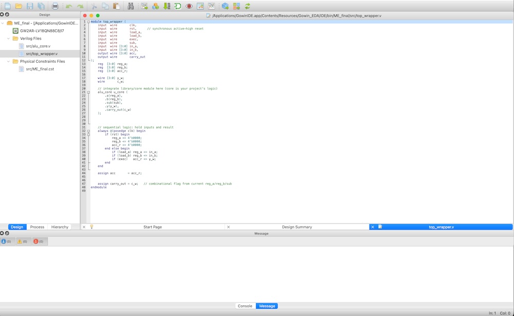
Add “New File”, and pasete the Verilog file that I wrote in session 04.
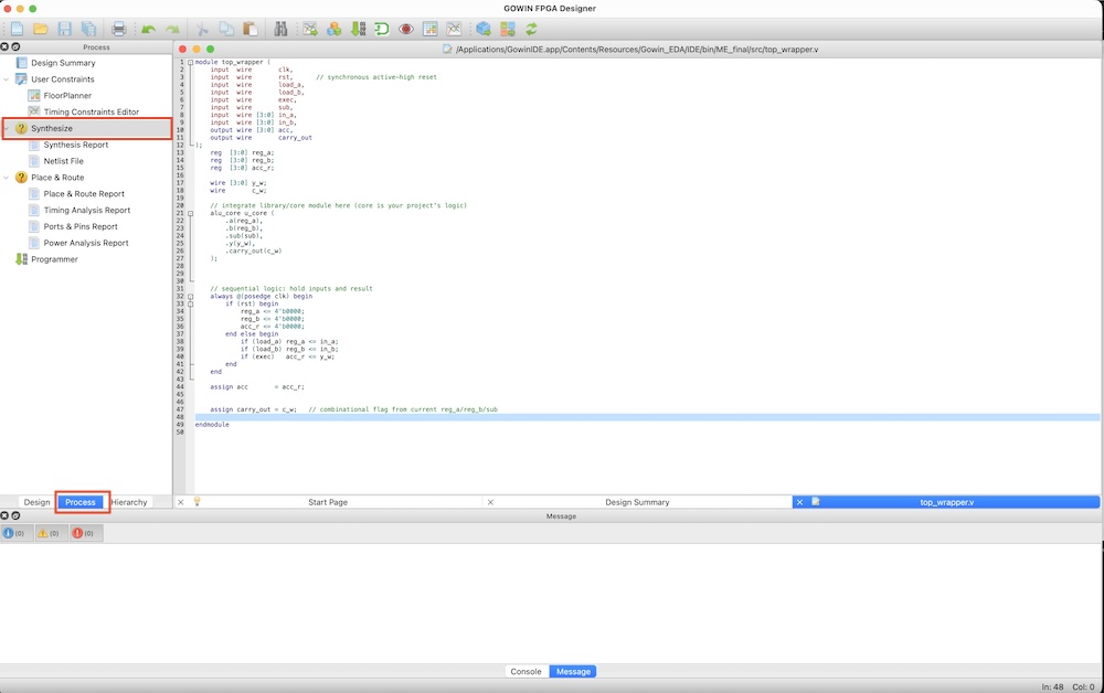
Click “Process” pain, then, click “synthesis”.
After finishing synthesis, then open “FloorPlanner”.
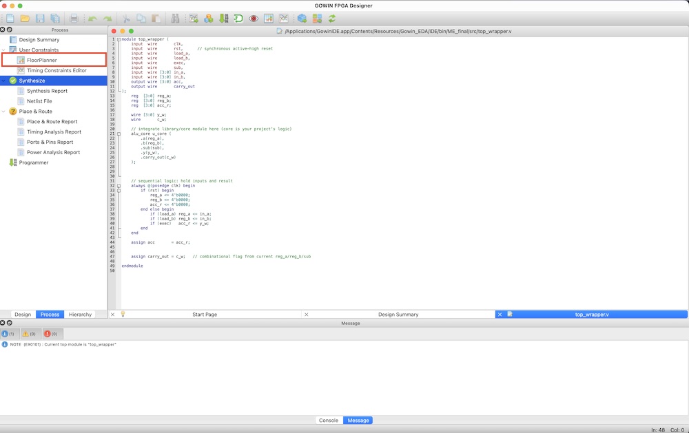
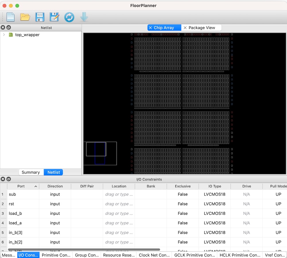
Floor Planner is to connect input/output of my chip design (by Verilog) to the FPGA board’s pinout.
Click “IO Constraints”, and we can defin the pin constraints. First time, it read my chip design’s input/output and we need to define which pin would be connected where in the Tang Nano 20K.
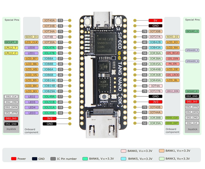
Here is the Tang Nano 20K’s pinout.
Also, it is important part to set the following constraints.
- IO type: Because we wrote verilog and synthesized with Sky130A pdks, the chip design is defined to work on 1.8v VDD, and most of FPGA dev board is worked in 3.3V VDD. So, we need to change all pin’s “IO Types” from “LVCOMS18” to “LVCMOS33”.
- Pull Mdode: I use switches and I also insert external pull-down register, so all input pin’s pull mode should be “none”.
- Use Internal LEDs: internal LEDS are defined in pin 15~17. I setupt those 17,18,19,20 as output pins and pull mode as “NONE”.
I defined the connection of my chip design to…
| Pin of my chip design | direction | Pin Number in Tang Nano 20K |
|---|---|---|
| clk | input | 15 |
| rst | input | 75 |
| sub | input | 77 |
| exec | input | 41 |
| load_a | input | 73 |
| load_b | input | 74 |
| ina[0] | input | 31 |
| ina[1] | input | 30 |
| ina[2] | input | 29 |
| ina[3] | input | 26 |
| inb[0] | input | 25 |
| inb[1] | input | 28 |
| inb[2] | input | 27 |
| inb[3] | input | 16 |
| carry_out | output | 48 |
| acc[0] | output | 17 |
| acc[1] | output | 18 |
| acc[2] | output | 19 |
| acc[3] | output | 20 |
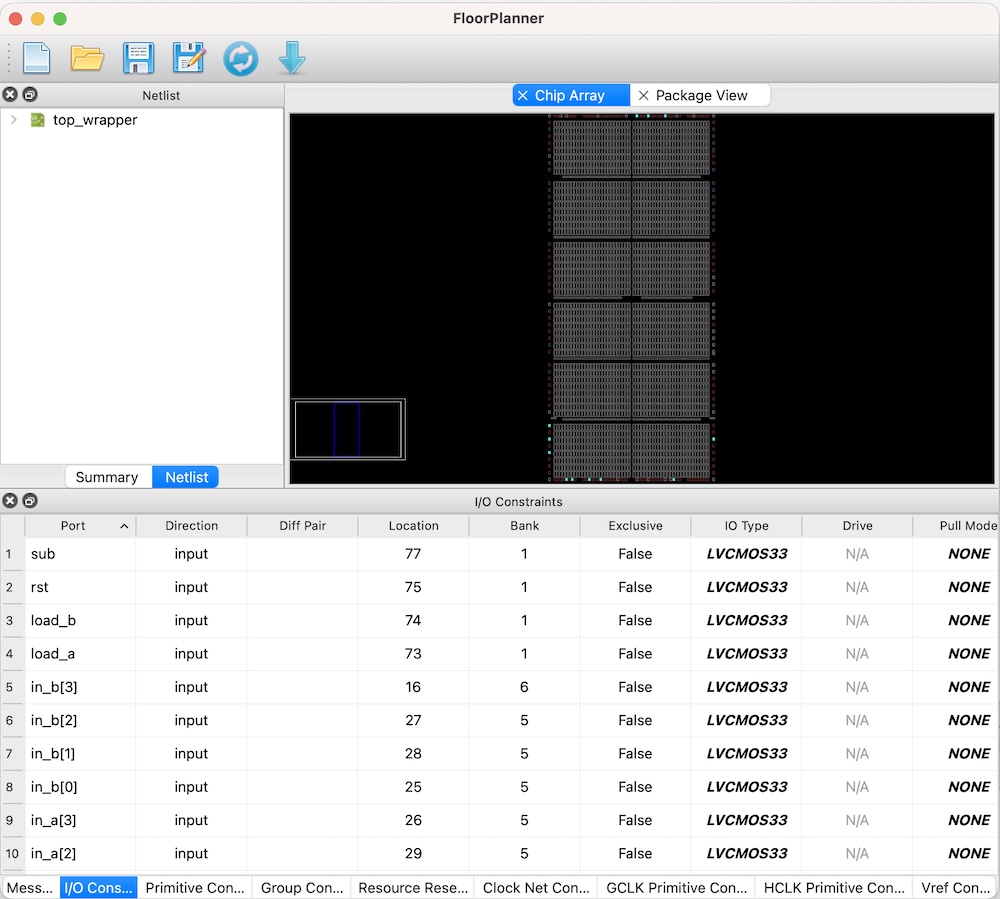
The final definintion are here. Save it into “**.cst” file.
Then, execute “Place & Route”. If something error occur, check again Floor Planner.
Now, it’s the time to write my chip design into FPGA. Click “Programmer”.
Fist, check the USB conenction. If my Tang Nano 20K is connected to my Mac, it could be found out here. Click “save” here.
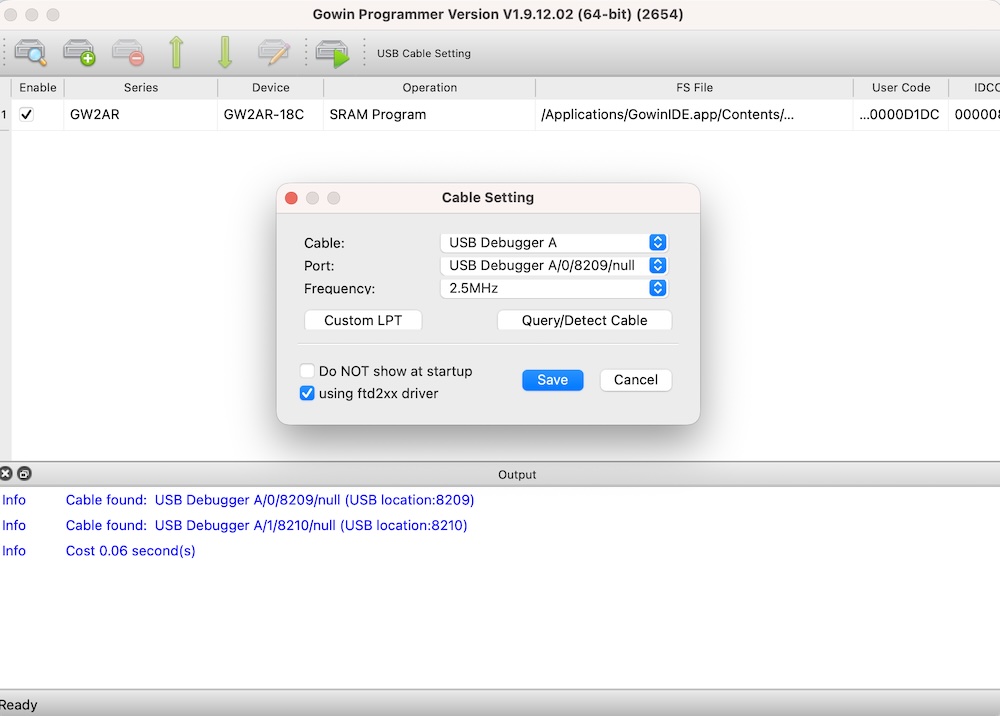
Then, you double-click “SRAM Program” in operation.
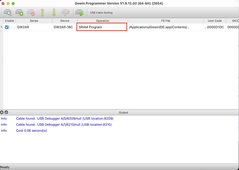
And, confirm that is setting as follow:
- Access mode: SRAM mode
- Operation: SRAM Program
Then, click “save”
Then, the SRAM file is downloaded and saved into local PC file. Because I use macos, I need to use external programmer (openloader), I did this operation.
So, again, double-click “SRAM Program”.
Next, I change the Access Mode and Operation as follow:
- Access mode: External Flash Mode
- Operation: exFlash Erase, Program, Verigy, thur GAO-Bridge
Then, click “save”.
Now, ready for programming. Click “Program” to start.
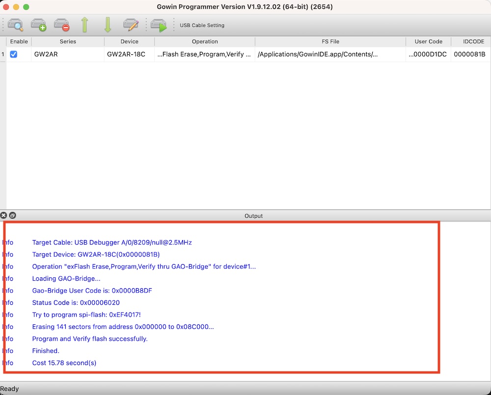
Programming is processing....
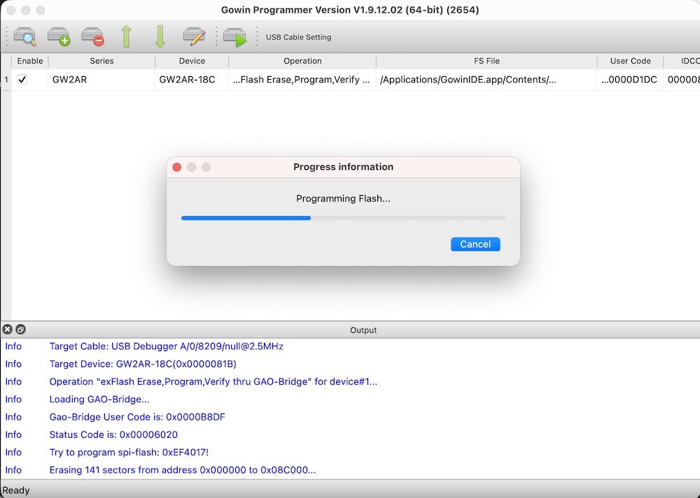
If the programming is finished, then the result is outcome in the console window.
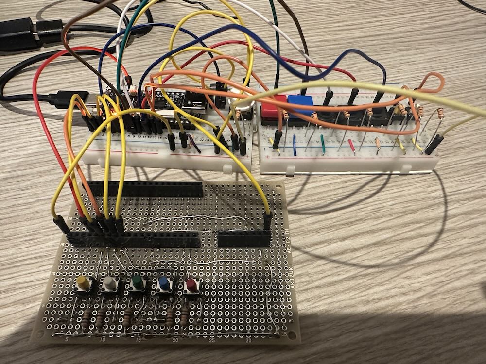
Then, I used breadboard and tact switches and one slide switched. Here is the wiring of switches to all input pins.
First, calcuiaton does not started, so all LEDs are blinked (make sure Tang Nano 20K internal LEDS are worked as active-low ). Here, from left ACC0 (first-bit),ACC1(second-bit), ACC2(third-bit), ACC3(4th-bit).
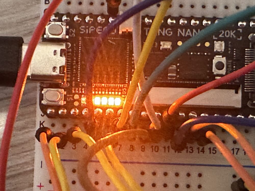
First, with pushing “Rst” button, push “clk” button one time, then release “Rst” button. Then registers are reseted.
Then, switch to adder mode. Here is the result of 3 + 5 = 8 (1000).
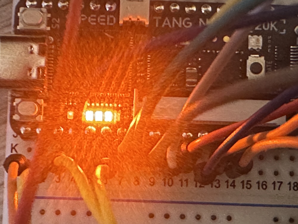
Then, swith to subtract mode. Here is the result of 8 - 5 = 3 (0011).
I could confirm my design chip is worked !
FPGA prottyping is very amayzing experience!