Final Project
Here is the summery of my first IC design project. Please also see each assignment document in detail.
Title: 4-bit adder/Subtractor with D-Flip Flop Register
Overview of the Project
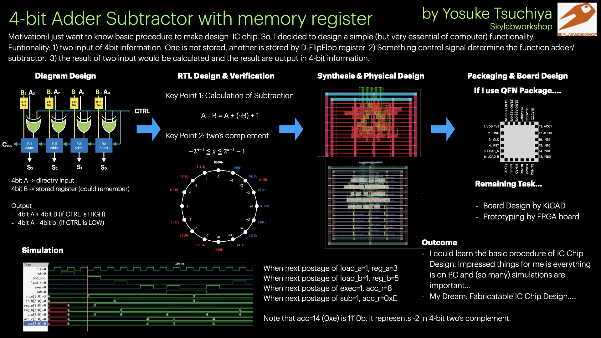
I just wanted to examine bsaic procedure to design IC chip. So, I decided to design a simple (but very essential of comptuter) funcationality.
This my IC Chip contains those fucntions:
1) two input of 4 bit information. Both inputs are stored by D Flip Flop register. 2) Control signal to determine the function of adder or subtractor. 3) the result of two input calculation is storeed into the registers and output it to 4-bit information
Basic Diagram
Here is the basic diagram of what I would design 4-bit calculator.

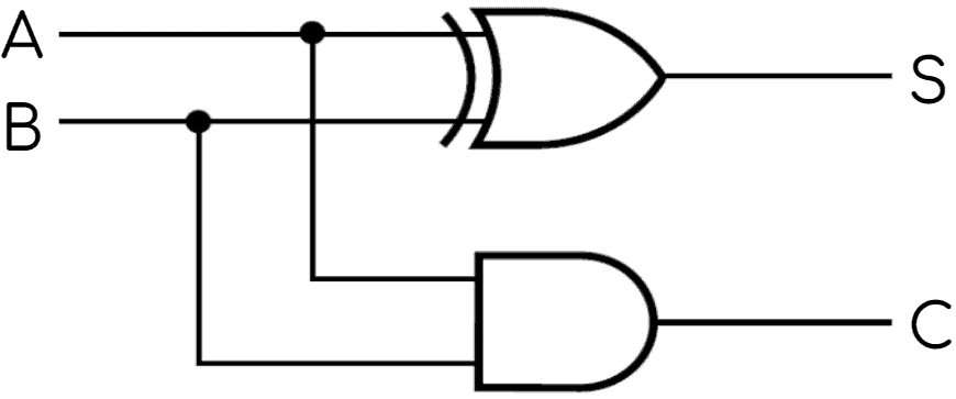
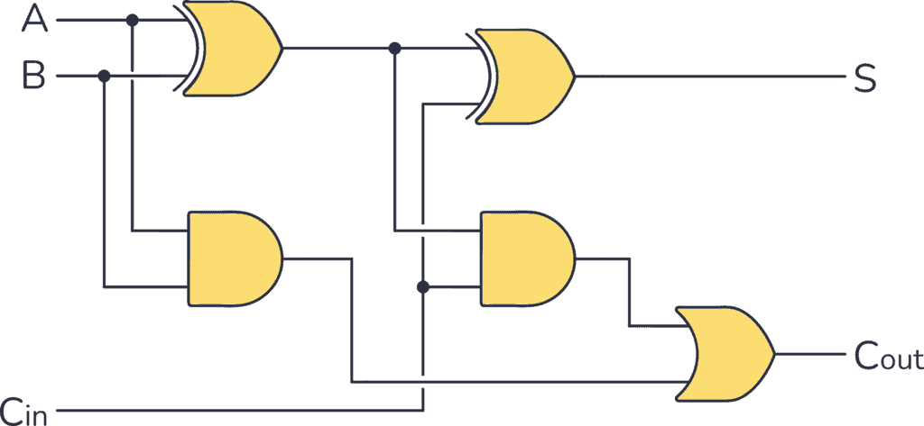
It consists of four Full adders. Each Full adders consist of Two Half Adder and And Gate with control signal.
- Half Adder: is a logic circuit that adds two 1-bit binary numbers (X and Y) and outputs the sum (Z) and a carry (C). It calculates the sum (Z) using an XOR gate and the carry (C) using an AND gate.
- Full Adder: is a basic logic circuit that adds three 1-bit binary inputs (input A, input B, and the carry from the lower digit) and outputs two bits: the sum of those digits () and the carry to the higher digit (). Unlike a half adder, it can account for the carry from the lower digit, enabling addition of any number of digits by connecting multiple units.
RTL Design and Verification
Pleae also see the document of session 04: RTL Design and Verification
Here is the Verilog of Arithmetic and Logic Unit (ALU) of my design IC chip
module alu_core (
    input  wire [3:0] a,
    input  wire [3:0] b,
    input  wire       sub,
    output wire [3:0] y,
    output wire       carry_out
);
    wire [3:0] b_xor;
    wire [4:0] sum;

    assign b_xor = b ^ {4{sub}};          // invert b when subtracting
    assign sum   = {1'b0, a} + {1'b0, b_xor} + {4'b0, sub};

    assign y         = sum[3:0];
    assign carry_out = sum[4];            // for subtraction, this is "no-borrow" flag
endmodule
This is a basic circuit block for adder/subtract calculation based on 4-bit adder. In this circuit, subtract is executed by two’s complement.
A - B = A + (~B) + 1
The following works as the top_wrapper. It define 14 input and 5 output (total 19 IO pins). reg_a and reg_b store the information that user input each number in 4-bit. load_a and load_b send the signal for
// top_wrapper.v
// Registers + core integration (simple "system")
// - load_a: latch in_a into reg_a
// - load_b: latch in_b into reg_b
// - exec  : compute reg_a +/- reg_b and store into acc

module top_wrapper (
    input  wire       clk,
    input  wire       rst,      // synchronous active-high reset
    input  wire       load_a,
    input  wire       load_b,
    input  wire       exec,
    input  wire       sub,
    input  wire [3:0] in_a,
    input  wire [3:0] in_b,
    output wire [3:0] acc,
    output wire       carry_out
);
    reg  [3:0] reg_a;
    reg  [3:0] reg_b;
    reg  [3:0] acc_r;

    wire [3:0] y_w;
    wire       c_w;

    // integrate library/core module here (core is your project's logic)
    alu_core u_core (
        .a(reg_a),
        .b(reg_b),
        .sub(sub),
        .y(y_w),
        .carry_out(c_w)
    );

    // sequential logic: hold inputs and result
    always @(posedge clk) begin
        if (rst) begin
            reg_a <= 4'b0000;
            reg_b <= 4'b0000;
            acc_r <= 4'b0000;
        end else begin
            if (load_a) reg_a <= in_a;
            if (load_b) reg_b <= in_b;
            if (exec)   acc_r <= y_w;
        end
    end

    assign acc       = acc_r;
    assign carry_out = c_w;   // combinational flag from current reg_a/reg_b/sub
endmodule
Then, here is the testbench for verifying the logical design of the chip.
// tb_top.sv
`timescale 1ns/1ps

module tb_top;
    logic       clk;
    logic       rst;
    logic       load_a, load_b, exec, sub;
    logic [3:0] in_a, in_b;
    wire  [3:0] acc;
    wire        carry_out;

    top_wrapper dut (
        .clk(clk),
        .rst(rst),
        .load_a(load_a),
        .load_b(load_b),
        .exec(exec),
        .sub(sub),
        .in_a(in_a),
        .in_b(in_b),
        .acc(acc),
        .carry_out(carry_out)
    );

    // 10ns period clock
    initial clk = 1'b0;
    always #5 clk = ~clk;

    initial begin
        $dumpfile("tb_top.vcd");
        $dumpvars(0, tb_top);

        // initialize
        rst    = 1'b0;
        load_a = 1'b0;
        load_b = 1'b0;
        exec   = 1'b0;
        sub    = 1'b0;
        in_a   = 4'h0;
        in_b   = 4'h0;

        // ---- reset ----
        @(negedge clk);
        rst = 1'b1;
        @(posedge clk);   // In this posedge works reset.
        @(negedge clk);
        rst = 1'b0;

        // ---- load A=3  ----
        @(negedge clk);
        in_a   = 4'd3;
        load_a = 1'b1;
        @(posedge clk);   // In this posedge, reg_a <= 3
        @(negedge clk);
        load_a = 1'b0;
        $display("[%0t] load_a done", $time);

        // ---- load B=5 ----
        @(negedge clk);
        in_b   = 4'd5;
        load_b = 1'b1;
        @(posedge clk);   // In this posedge, reg_b <= 5
        @(negedge clk);
        load_b = 1'b0;
        $display("[%0t] load_b done", $time);

        // ---- ADD: 3 + 5 = 8 ----
        @(negedge clk);
        sub  = 1'b0;
        exec = 1'b1;
        @(posedge clk);   // In this posedge, acc <= 8
        @(negedge clk);
        exec = 1'b0;
        @(posedge clk);   // wait 1 clock for displaying
        $display("[%0t] ADD 3+5 => acc=%0d (0x%0h), carry=%0b", $time, acc, acc, carry_out);

        // ---- SUB: 3 - 5 = -2 = 0xE ----
        @(negedge clk);
        sub  = 1'b1;
        exec = 1'b1;
        @(posedge clk);   // In this postage acc <= 0xE
        @(negedge clk);
        exec = 1'b0;
        @(posedge clk);
        $display("[%0t] SUB 3-5 => acc=%0d (0x%0h), carry(no-borrow)=%0b", $time, acc, acc, carry_out);

        // ---- Change external input (not loaded ----
        @(negedge clk);
        in_a = 4'd9;
        in_b = 4'd2;

        // reg_a/reg_b is still 3,5, so acc is still 8
        @(negedge clk);
        sub  = 1'b0;
        exec = 1'b1;
        @(posedge clk);
        @(negedge clk);
        exec = 1'b0;
        @(posedge clk);
        $display("[%0t] HOLD-CHECK => acc=%0d (0x%0h) (expected 8)", $time, acc, acc);

        // ---- Only update B: 3 + 2 = 5 ----
        @(negedge clk);
        load_b = 1'b1;
        @(posedge clk);   // In this posedge, reg_b <= 2
        @(negedge clk);
        load_b = 1'b0;
        $display("[%0t] load_b(2) done", $time);

        @(negedge clk);
        exec = 1'b1;
        @(posedge clk);   // In this posedge, acc <= 5
        @(negedge clk);
        exec = 1'b0;
        @(posedge clk);
        $display("[%0t] ADD 3+2 => acc=%0d (0x%0h)", $time, acc, acc);

        repeat (2) @(posedge clk);
        $finish;
    end
endmodule
Then, run the following commands, and got the result.
(base) yosuke@ysk-M1Pro design % iverilog -g2012 -o sim_addr-subtract.vvp tb_top.sv alu_core.v top_wrapper.v
(base) yosuke@ysk-M1Pro design % vvp sim_addr-subtract.vvp
VCD info: dumpfile tb_top.vcd opened for output.
[40000] load_a done
[60000] load_b done
[85000] ADD 3+5 => acc=8 (0x8), carry=0
[105000] SUB 3-5 => acc=14 (0xe), carry(no-borrow)=0
[135000] HOLD-CHECK => acc=8 (0x8) (expected 8)
[150000] load_b(2) done
[175000] ADD 3+2 => acc=5 (0x5)
tb_top.sv:118: $finish called at 195000 (1ps)
Finally, show the waveform.
gtkwave tb_top.vcd
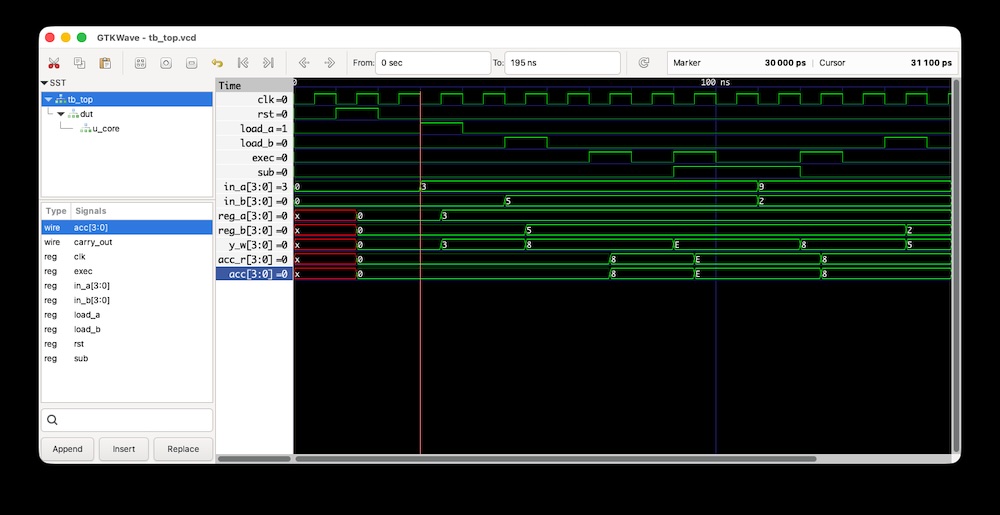
- When next postage of load_a=1, reg_a=3
- When next postage of load_b=1, reg_b=5
- When next postage of exec=1, acc_r=8
- When next postage of sub=1, acc_r=0xE
Note that acc=14 (0xe) is 1110b, it represents -2 in 4-bit two’s complement.
I could verified the logical chip design.
Synthesis and Physical Fabrication
Please also see session 06 document
I used “yosys” for sysnthesis of my IC design. The statistics of my synthesis is here:
7. Printing statistics.

=== top_wrapper ===

        +----------Local Count, excluding submodules.
        |
       39 wires
       60 wire bits
       15 public wires
       36 public wire bits
       10 ports
       19 port bits
       36 cells
       12   sky130_fd_sc_hd__dfxtp_1
       12   sky130_fd_sc_hd__mux2i_1
       12   sky130_fd_sc_hd__nor2_1
        1 submodules
        1   alu_core

=== alu_core ===

        +----------Local Count, excluding submodules.
        |
       15 wires
       28 wire bits
        6 public wires
       19 public wire bits
        5 ports
       14 port bits
       14 cells
        3   sky130_fd_sc_hd__maj3_1
        1   sky130_fd_sc_hd__mux2_1
        6   sky130_fd_sc_hd__xnor2_1
        4   sky130_fd_sc_hd__xor2_1

=== design hierarchy ===

        +----------Count including submodules.
        |
       50 top_wrapper
       14 alu_core

        +----------Count including submodules.
        |
       54 wires
       88 wire bits
       21 public wires
       55 public wire bits
       15 ports
       33 port bits
        - memories
        - memory bits
        - processes
       50 cells
       12   sky130_fd_sc_hd__dfxtp_1
        3   sky130_fd_sc_hd__maj3_1
        1   sky130_fd_sc_hd__mux2_1
       12   sky130_fd_sc_hd__mux2i_1
       12   sky130_fd_sc_hd__nor2_1
        6   sky130_fd_sc_hd__xnor2_1
        4   sky130_fd_sc_hd__xor2_1
        1 submodules
        1   alu_core
And, I could find my IC has…
| Metric | Value |
|---|---|
| Total Cells | 50 |
| Flip-flops | 12 |
| Muxes | 13 |
| XOR/XNOR | 10 |
And, there are No latches warning, so wrote an output as netlist.
Then, I used “openroad” for placing and routing of my chip design. Openroad declare no errors and I could generated the gds file.
Then, my IC design physical layout has come… I was deeply moved to see this.

Operoad does not output any error notifications. So, I passed the physical design verification.
Final Packaging and Prototyping
Please also see session 07 docs for details of my chip descriptions and evaluation.
Pin Assign of the Chip
It would packaged with QFN package…
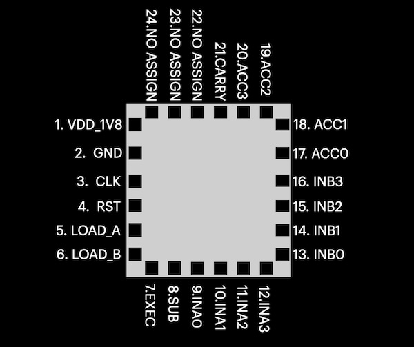
Pin assing description here.
| pin no. | pin name | direction | description |
|---|---|---|---|
| 1 | VDD_1V8 | Power | 1.8 V power supply for the chip core. |
| 2 | GND | Power | Ground reference |
| 3 | CLK | Input | System clock input. All register updates occur on the rising edge of this clock. |
| 4 | RST | Input | Synchronous reset input. Clears internal registers (reg_a, reg_b, acc) to zero when asserted. |
| 5 | LOAD_A | Input | Loads the external input INA[3:0] into register A on the next rising clock edge. |
| 6 | LOAD_B | Input | Loads the external input INB[3:0] into register B on the next rising clock edge. |
| 7 | EXEC | Input | Executes the selected arithmetic operation on the next rising clock edge and stores the result into the accumulator register. |
| 8 | SUB | Input | Operaton select. 0= addition, 1= subtraction |
| 9 | INA0 | Input | Bit 0 of 4-bit operand A external input |
| 10 | INA1 | Input | Bit 1 of 4-bit operand A external input |
| 11 | INA2 | Input | Bit 2 of 4-bit operand A external input |
| 12 | INA3 | Input | Bit 3 of 4-bit operand A external input |
| 13 | INB0 | Input | Bit 0 of 4-bit operand B external input |
| 14 | INB1 | Input | Bit 1 of 4-bit operand B external input |
| 15 | INB2 | Input | Bit 2 of 4-bit operand B external input |
| 16 | INB3 | Input | Bit 3 of 4-bit operand B external input |
| 17 | ACC0 | Output | Bit 0 of 4-bit accumulator output |
| 18 | ACC1 | Output | Bit 1 of 4-bit accumulator output |
| 19 | ACC2 | Output | Bit 2 of 4-bit accumulator output |
| 20 | ACC3 | Output | Bit 3 of 4-bit accumulator output |
| 21 | CARRY | Output | Carry output for addition, or no-borrow flag for subtraction. |
| 22 | NC | - | No connection |
| 23 | NC | - | No connection |
| 24 | NC | - | No connection |
Design of PCB for Chip Evaluation
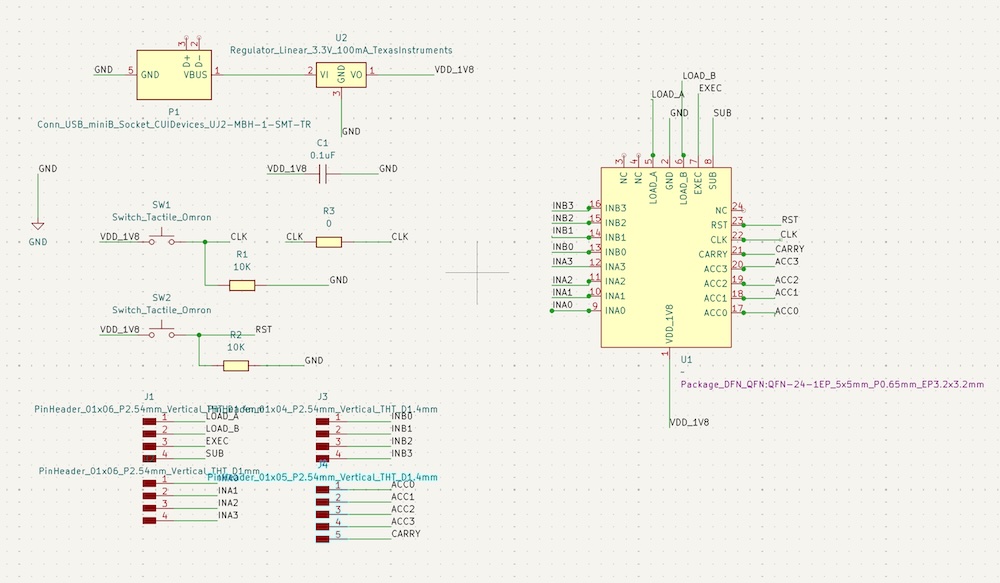
I tried to design Evaluation board of my chip with KiCAD.
Here is the schema of the eval board.
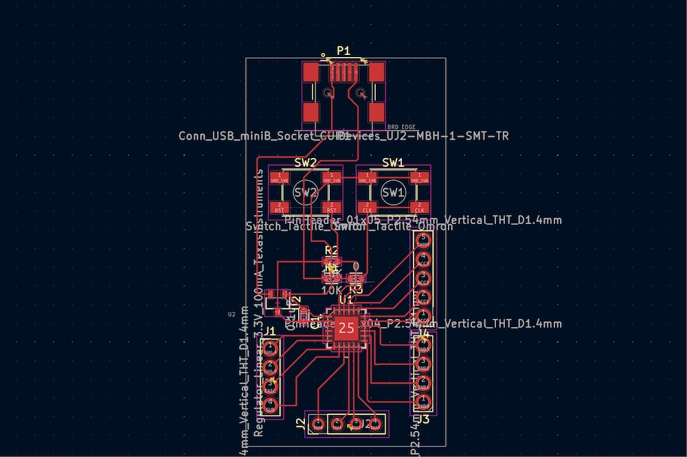
And this is the PCB design of the eval board.
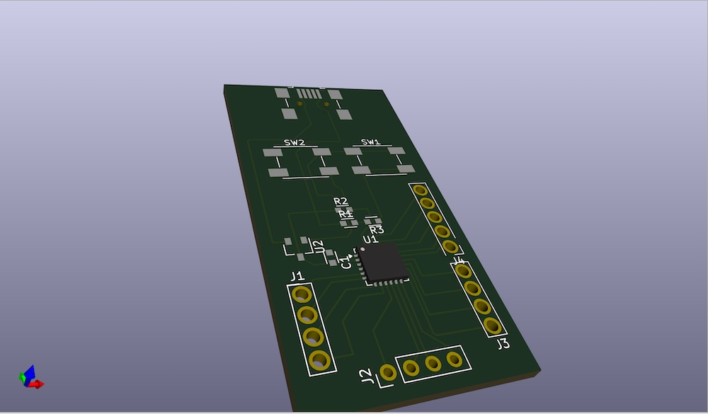
Then, 3D view would be come out.
Test by FPGA Prototyping
I did FPGA Prototyping using Tang Nano 20K for testing my design would work or not.
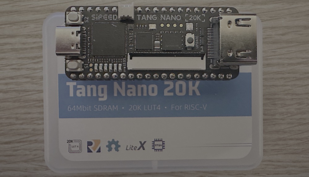
I connected my chip design to the following pins of Tang Nano 20K.
| Pin of my chip design | direction | Pin Number in Tang Nano 20K |
|---|---|---|
| clk | input | 15 |
| rst | input | 75 |
| sub | input | 77 |
| exec | input | 41 |
| load_a | input | 73 |
| load_b | input | 74 |
| ina[0] | input | 31 |
| ina[1] | input | 30 |
| ina[2] | input | 29 |
| ina[3] | input | 26 |
| inb[0] | input | 25 |
| inb[1] | input | 28 |
| inb[2] | input | 27 |
| inb[3] | input | 16 |
| carry_out | output | 48 |
| acc[0] | output | 17 |
| acc[1] | output | 18 |
| acc[2] | output | 19 |
| acc[3] | output | 20 |
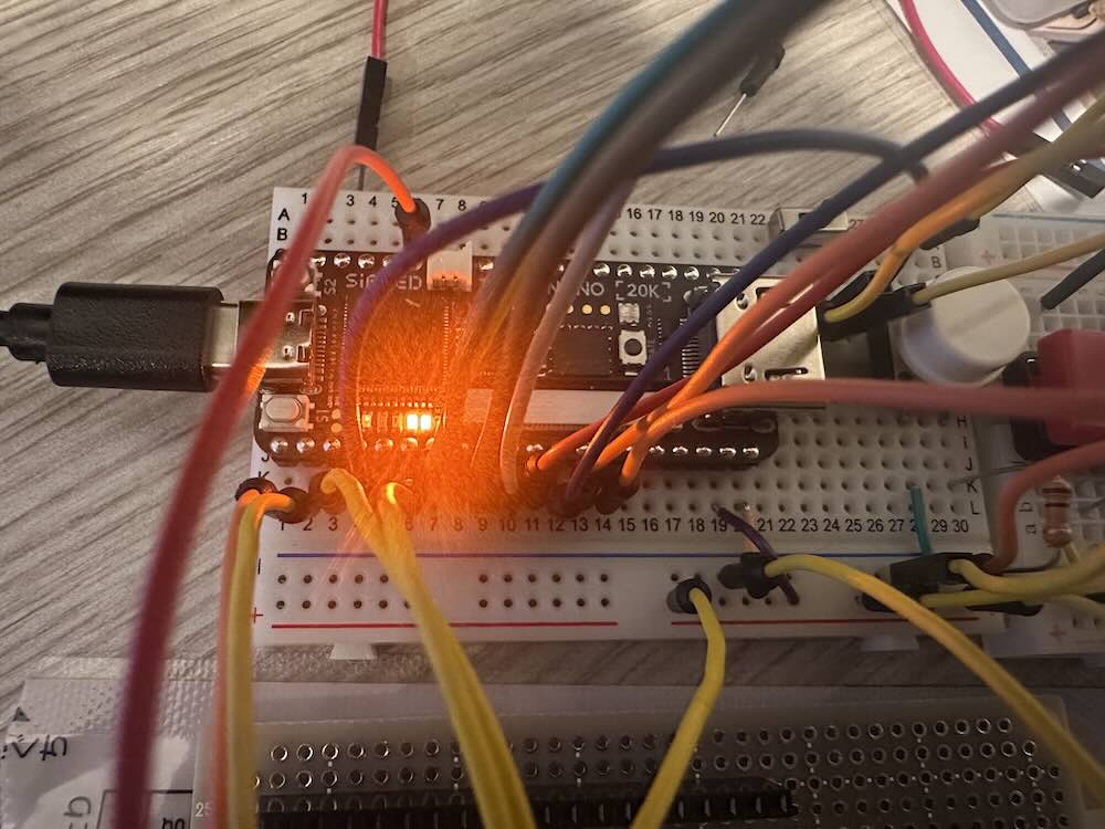
Then, flashed my design into FPGA board and make the following breadboard circuit for calculation test.
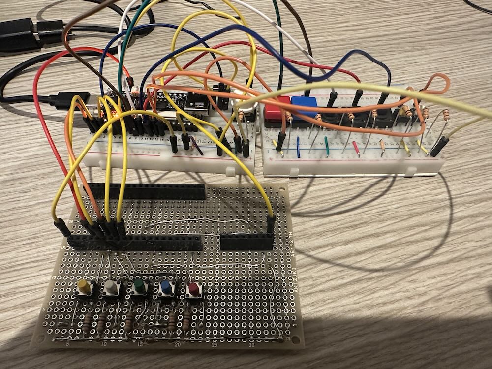
First, calcuiaton does not started, so all LEDs are blinked (make sure Tang Nano 20K internal LEDS are worked as active-low ). Here, from left ACC0 (first-bit),ACC1(second-bit), ACC2(third-bit), ACC3(4th-bit).
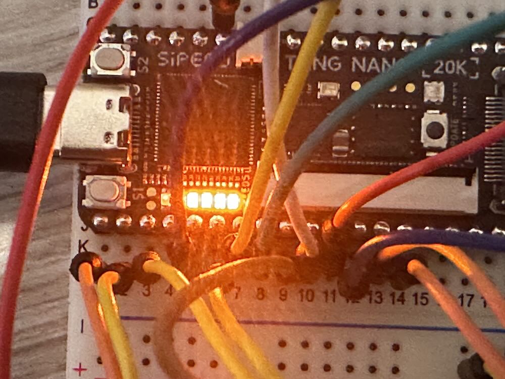
First, with pushing “Rst” button, push “clk” button one time, then release “Rst” button. Then registers are reseted.
Then, switch to adder mode. Here is the result of 3 + 5 = 8 (1000).
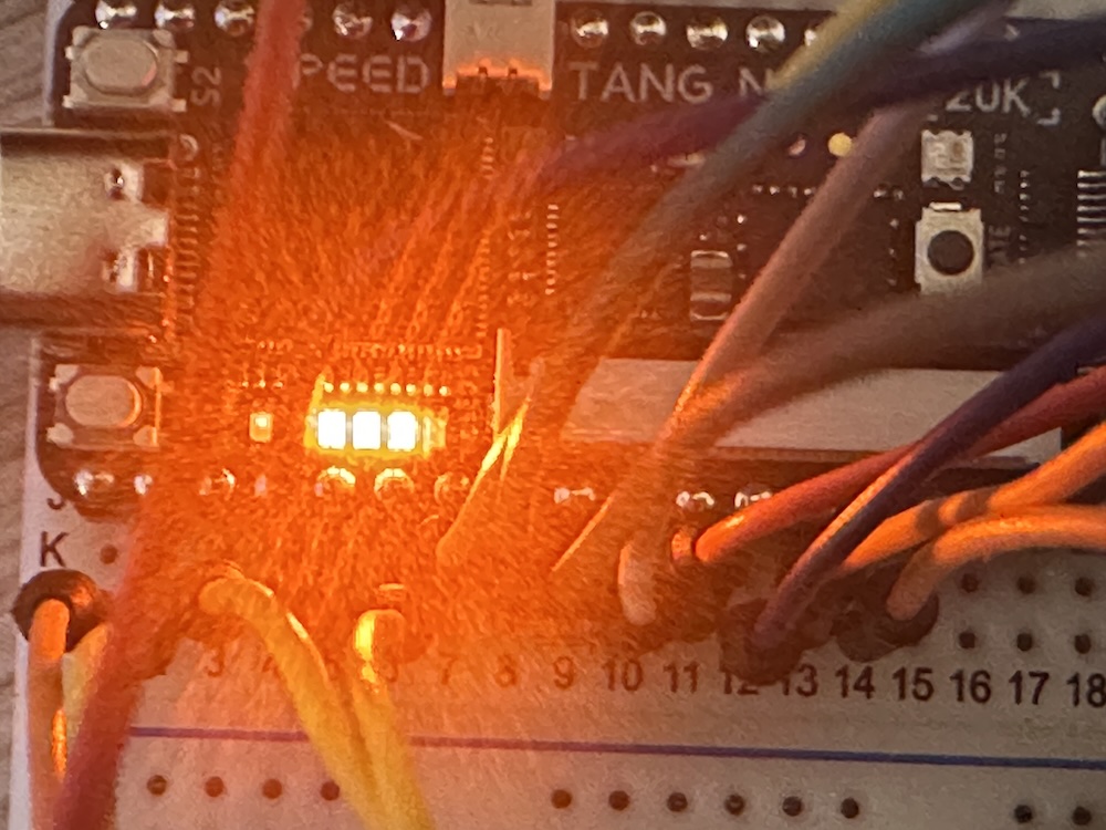
Then, swith to subtract mode. Here is the result of 8 - 5 = 3 (0011).
I could confirm my design chip is worked!
Acknowledgement
I would like to thanks all the class mate and instructors of Fab Future - Microelctronics all over the world. Especially, thanks for Rico for sharing useful knowledges and instructions. Also, I would like to thanks to Þórarinn for his nice and useful information.
I also would like to thanks for ChatGPT. Some of this documentations are proofreaded by him/her.