Session 4 > Fabrication Basics
Research
It was late and I was tired…so the class with Alex Wynn was a bit of a blur. I will have to review the video to understand more deeply all the content of the session. What stuck with me from the session was the description of nanoscale circuitry in stacked layers.
So while I wait for the class video to be uploaded, my classmate and friend Thorarinn posted this in our mattermost channel > 3D Printable Inverter Model
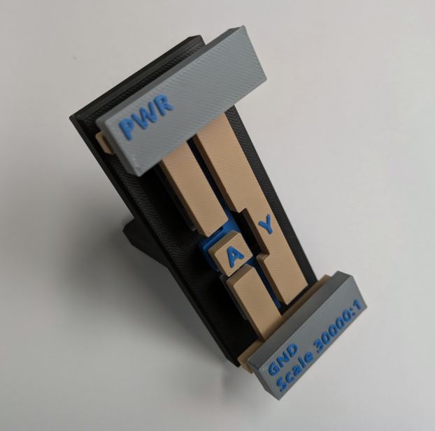
A 3D Model we can print and get a tactile and intuitive understanding of nanoscale circuitry. I was sold. Press print, let’s go!!
Class Review
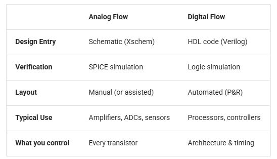
Analog > Layout > Design
Transistors > SPICE > Verilog
Digital design abstracts away the physics, but the physics is still there.
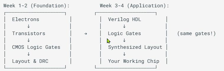
Alex gave us a roadmap of where we have been and where we are going (in this course). Up till now, we have been learning the fundamental knowledge (electrons, transistors, CMOS Logic gates) and tools needed to do what this course was meant to teach. From this point forward, we dive fully into the digital realm to progress towards a fabricatable (rudimentary) chip design.
- SPICE is good up until up to about 1000 devices
-
Analog Flow vs Digital Flow
-
Verilog HDL code describes logic that exists as hardware gates and transistors on silicon (or on FPGA)
Layout Tools
- K-layout (used for what? vs XSchem?)
File Format
- GDS > most common, binary format
- Oasis > 10x more compact than GDS
Layout Procedure 1. Draw schematic > schematic capture: Xschem, LTspice 2. Convert to HDL Netlist 3. Run Simulations 4. View Waveforms
Open Source Analog ASIC design
LVS > Layout vs Schematic, the difference between schematic and actual physical devices. Schematic vs Layout Netlists!
Standard Cells > pre-designed, pre-verified layout blocks for common logic gates
Gotta admit, even after the second time through the lecture, I am still not certain as to what I am supposed to do and how to do it.
Design Rules
“DRC ensures that your layout meets the physical constraints of the fabrication process…because of lithography resolution limits, etching characteristics and reliability requirements.”
Example key Geometry Design Rules include:
- Minimum (metal pad) Width
- Minimum Spacing (between metal pads)
- Via (metal) Enclosure Width
- Metal Density (within a specific area)
Example Reliability Rules
- Antenna Rules > disperse charge on long wires with diodes or vias
- Electromigration Rules > minimum wire widths depending on expected current to avoid atoms migration
Layout Versus Schematic (LVS) Check
- extracts Netlist and compares it to the original physical geometry
Process Development Kit (PDK)
- all specifications needed for designing for a specific Fab process.

Multilayered Metal
Modern processors, in order to get more transistors in a smaller space, stacks metal layers 3-dimensionally.
Terminology
HDL > Hardware Description Language, hardware as code instead of drawn schematics
Yosys > is a framework for Verilog RTL, an open source synthesis tool that converts Verilog code into gate-level logic…a compiler for hardware (ChatGPT)
RTL > Register Transfer Level, a level of abstraction that describe how data moves between (flip-flop) registers and how combinational logic transforms that data. The Abstraction Heirarchy: Transistor Level (lowest, PMOS/NMOS) > Gate Level (after Yosys, NAND, NOR, Flip-Flops) > RTL (registers, cominational logic, clocked behavior, synthesizable) > Behavioral Level (high-level, “what should happen?”) (ChatGPT)
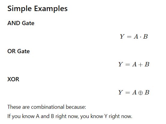
Combinational Logic > Logic where the output depends on only the current inputs. No memory. No clock. No flip-flops. No latches No previous state. Just pure logic. Has Propagation Delays, Rise/Fall Times, Gate Delay. Versus Sequential Logic (has memory). (ChatGPT)
FPGA > Field Programmable Gate Array, a reprogrammable (using Hardware description language, Verilog HDL) integrated circuit
ASIC > Application Specific Integrated Circuit, not reprogrammable after initial programming, designed for specific tasks
Assignment Work
[x] Block Diagram: > Sketch your project’s architecture (make a Flow Chart) showing major modules and data flow (e.g. Pocket Synth: button input > tone selector > oscillator > PWM output)
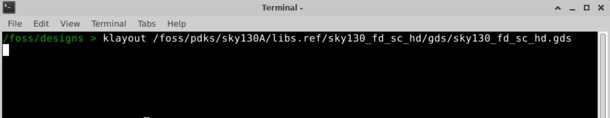
[x] Explore a Standard Cell: Open sky130 standard cell library in Klayout and find an inverter (sky130_fd_sc_hd__inv_1). Identify metal, poly, and diffusion layers
[ ] Connect the Dots: Pick one block from your diagram > what standard cells might implement it? (e.g. “counter” needs flip-flops, “tone selector” needs muxes)
My understanding of the 3 assignments:
- Decide on a project and draw a flow diagram for it.
- Poke around KLayout and learn how to navigate around it.
- Choose a block from the flow diagram and choose a Standard Cell that might implement it.
Block Diagram
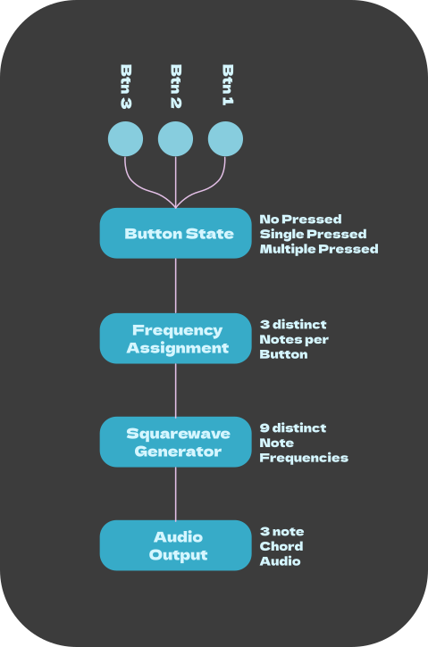
I am a huge fan of synthesizers. To learn electronics after graduating from Fabacademy, I have been learning and building Analog Synthesizer modules (oscillators, filters, amplifiers, etc.) using discrete electronic components.
While I am still trying to understand what it is we are expected to produce at the end of this course, I very much want to do something with synthesizers.
Inspired by the example from week 1, the Pocket Synth, I am thinking to do something along those lines. A small keyboard that plays chords, not just notes. So the functional diagram would look something like this…
Explore a Standard Cell in KLayout
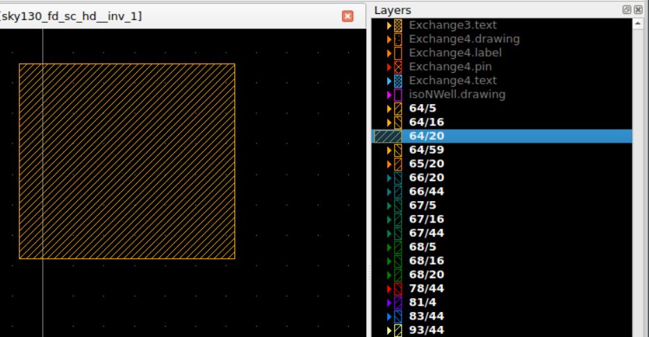
Mission: > find an inverter “sky130_fd_sc_hd__inv_1”


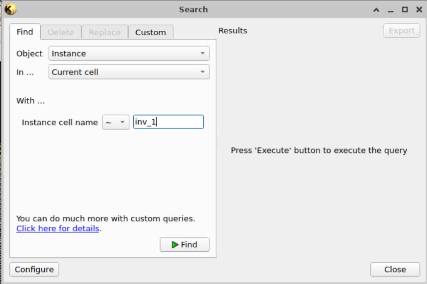
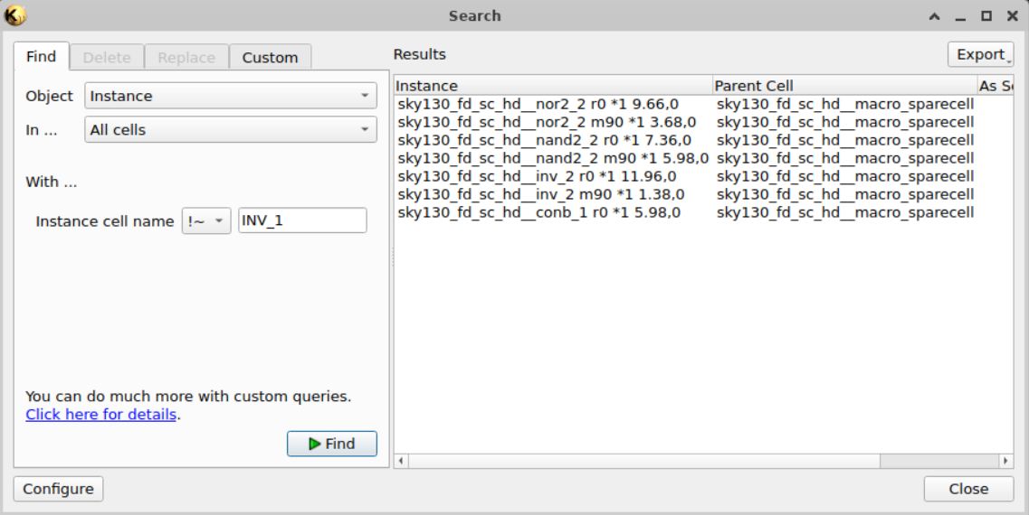
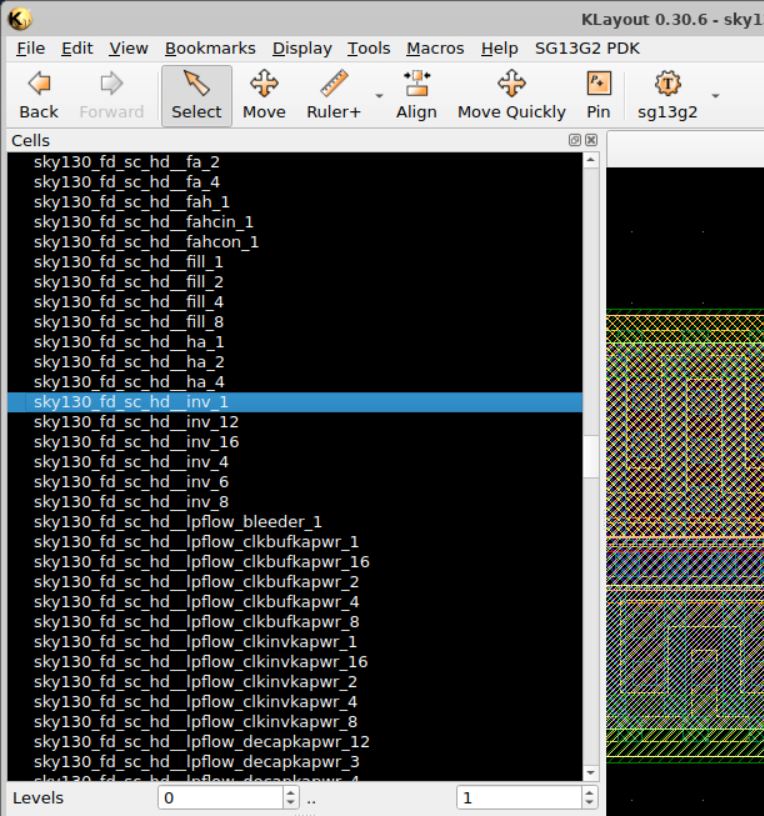
I followed the homework instructions (and hints) and the above was as far as I got. I thought to try something new and got the following:

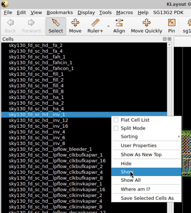

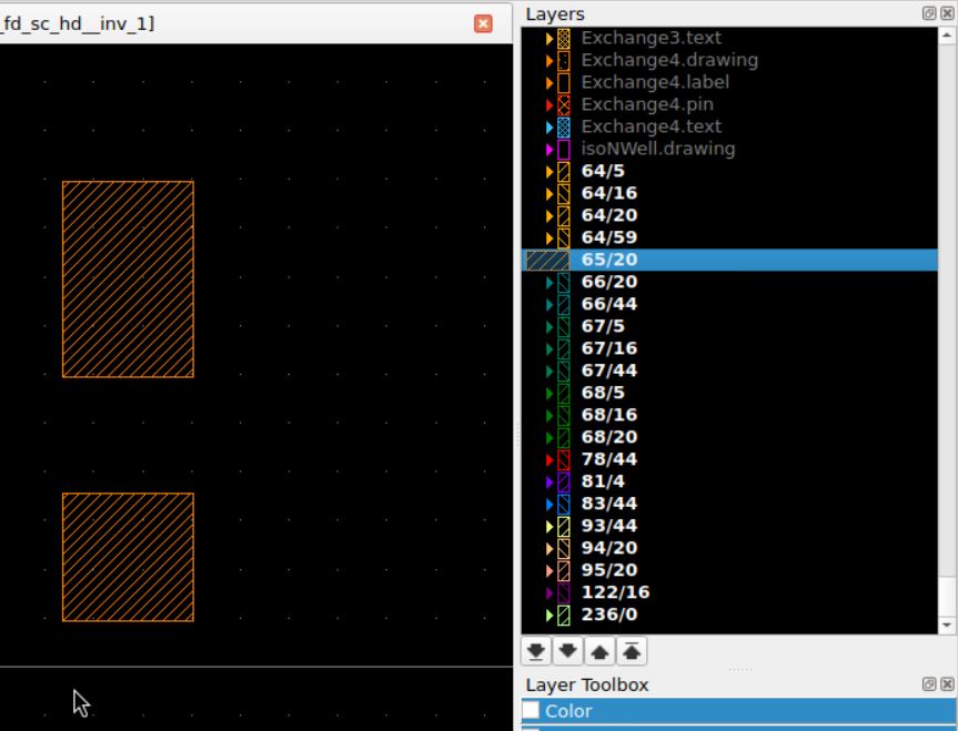
I think I managed to open the INV_1 file. Now to figure out how to find the Metal, Poly and Diffusion layers. On the right side, there are lots of names with the word ‘Metal’ in it. But one was highlighted, so I hid everything else
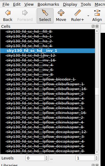
Right mouse clicking on ‘INV 1’ and choosing ‘Show as New Top’, I got this:
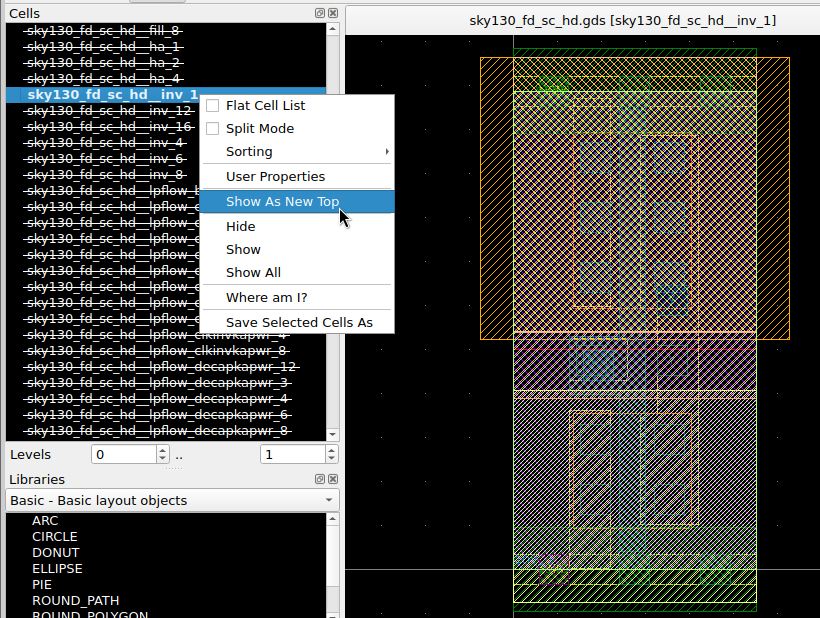
I think I am looking at the Inverter isolated from the rest of the circuit.
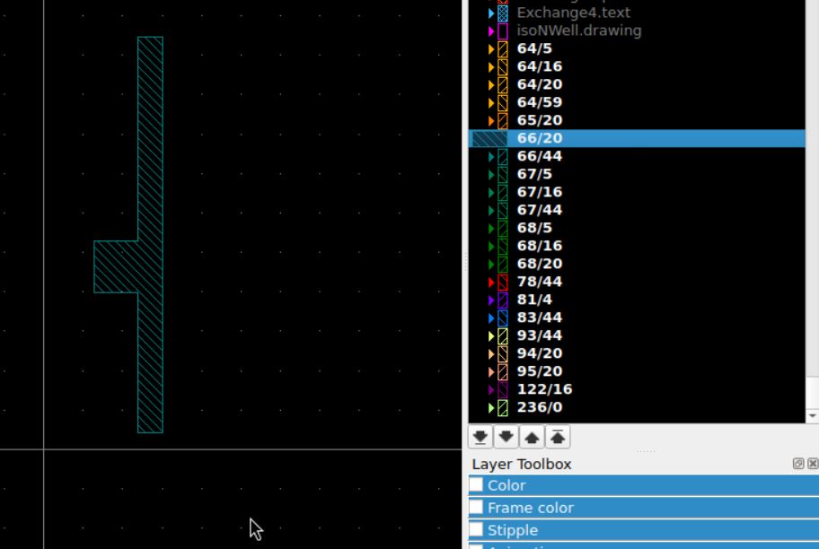
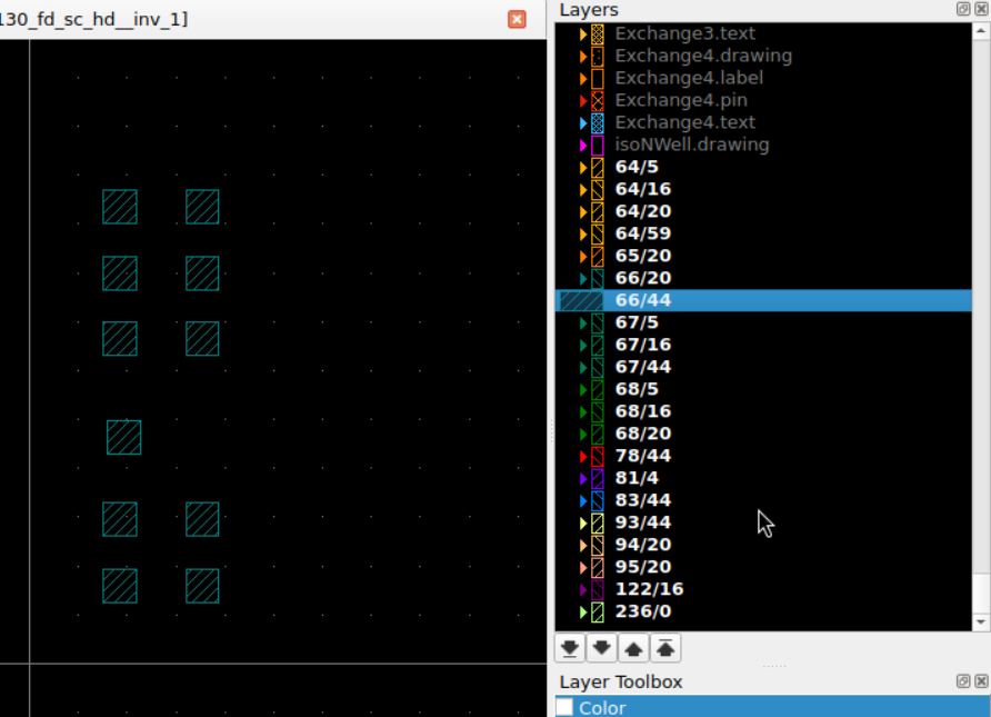
Next I moved to the Layer window, hiding every layer first…then unhiding them one by one. And discovered that the only layers that produced anything were the numbered layers at the bottom (with bold white text).
64/20
65/20
66/20
66/44
I notice that these layers are color coded. I will follow up on these colors later…
67/5 & 67/16 & 67/44
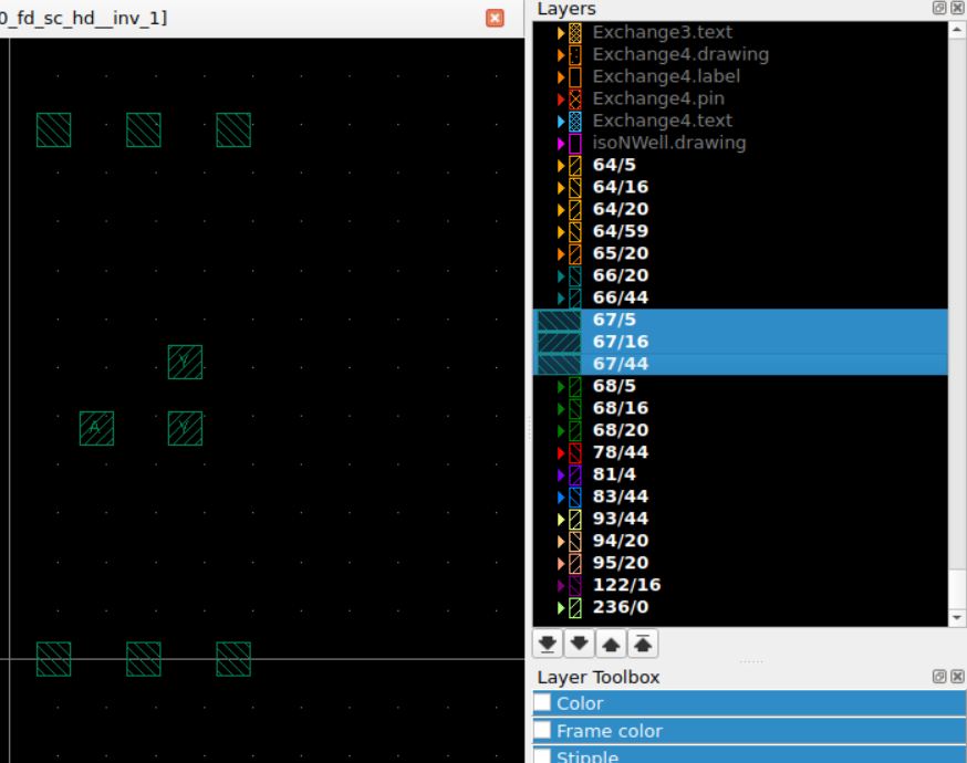
68/5 & 68/16 & 68/20
Now I am wondering what the numbers represent…
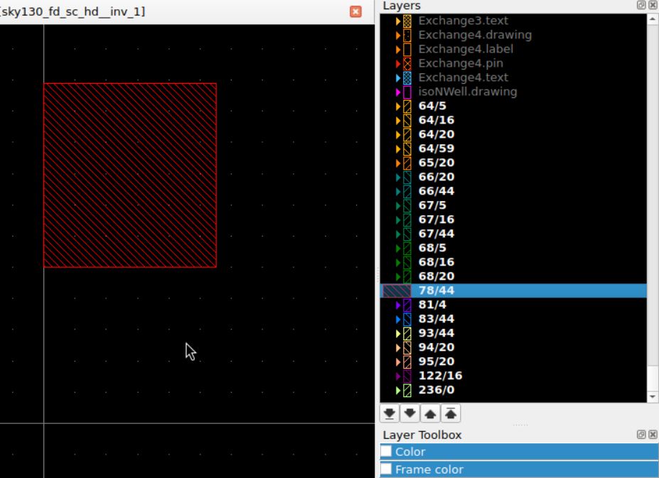
78/44
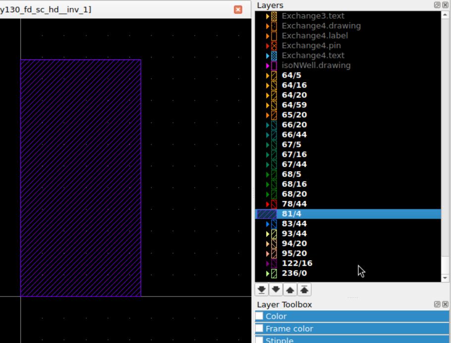
81/4
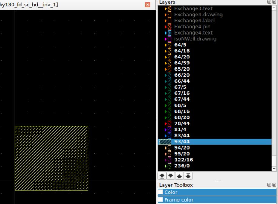
93/44
94/20
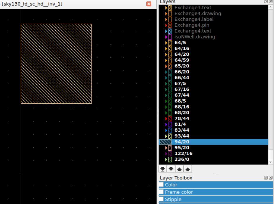
95/20
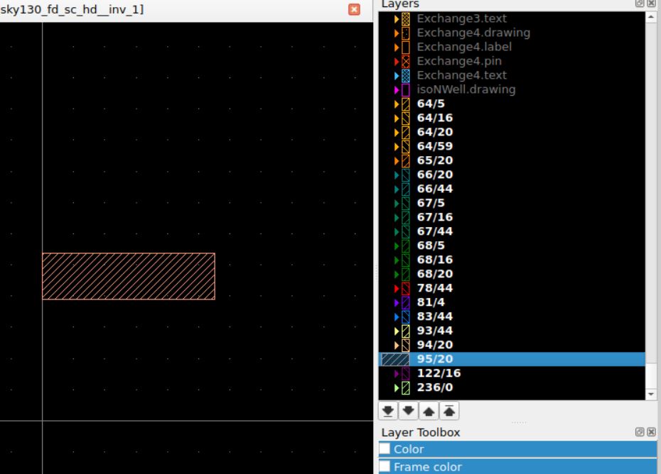
120/16
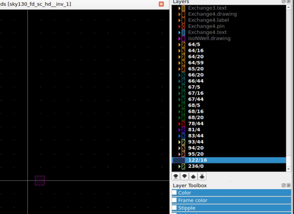
236/0
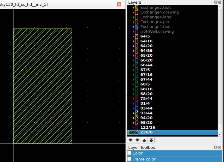
Ok, now to figure out which of these layers is Metal, Poly and Diffusion. Scouring the internet, I chanced on this Klayout documentation.
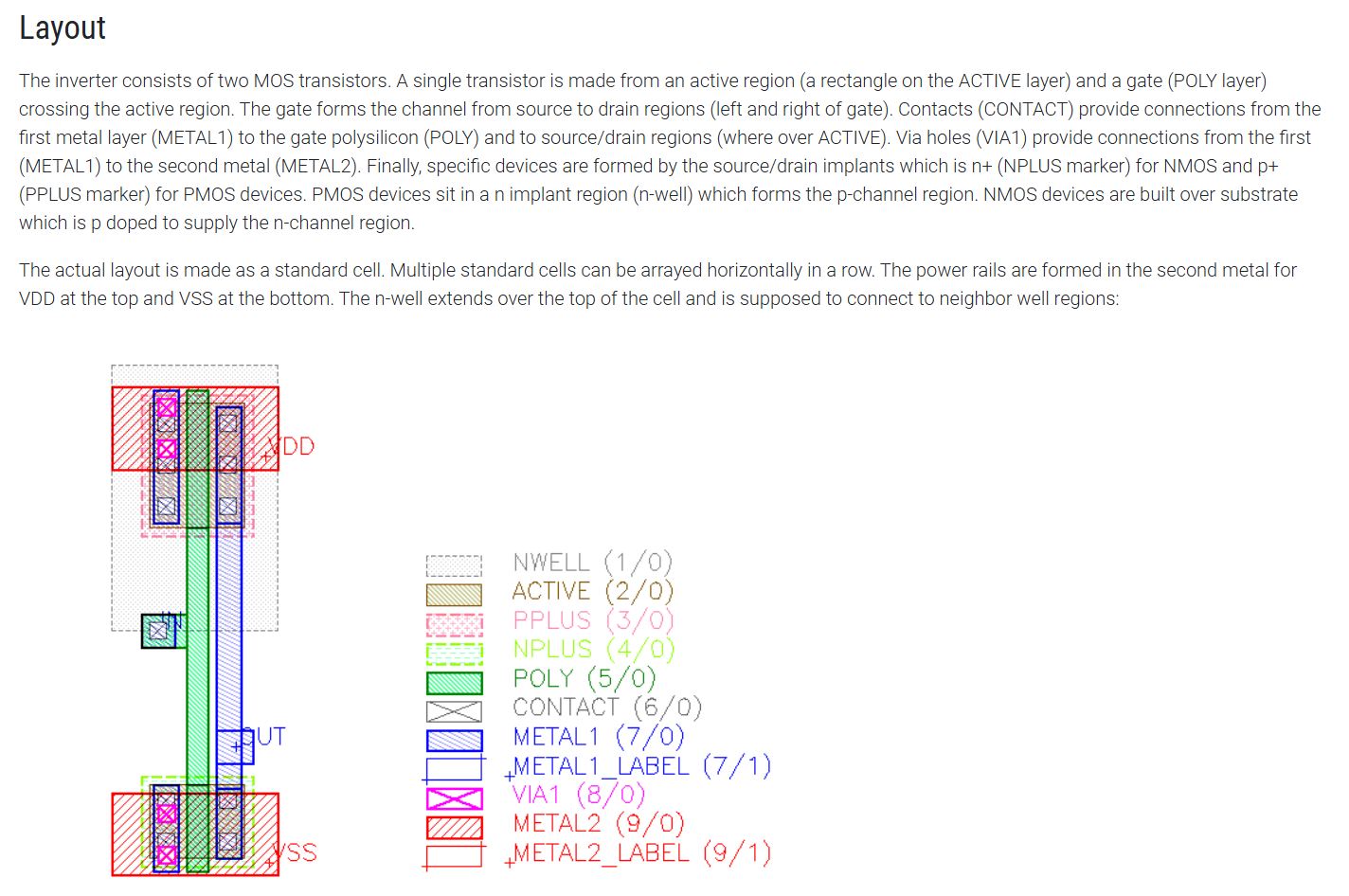
This should help me decipher the images above.
Choose a Standard Cell for a Flow Block
Looking at the Pocket Synth code, I focused on the Tone Generator section.
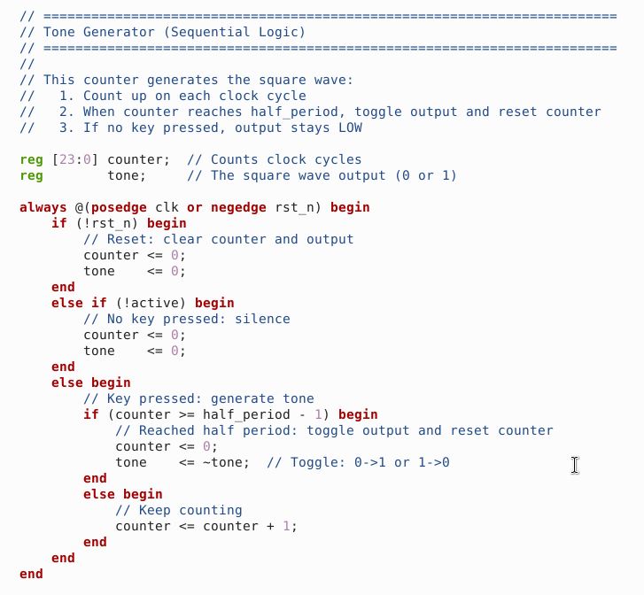
I understand that there is a counter that increments with each clock cycle, up to a specific value…then resets. This counter is used to define note frequency. Each note has a different frequency, so a different counter max value.
Querying ChatGPT for what Standard Cell would be required to create a counter, it responded with the following:
- D-type Flip-Flops > stores counter state, one needed for each note
- Add Logic > increments the value upward
- Comparator Logic > detects threshold value reached
- Multiplexor Logic > chooses between the different threshold values (then resets)
- Output Toggle Logic > to generate Square Wave
- Basic Logic > NAND, NOR, INV, XOR, XNOR, AND, OR
References
KLayout
Klayout Documentation
Klayout LVS