Session 7 > Packaging & Board Design
Class Notes
- The produced chip will require “Packaging”…to give it (mechanical, chemical, thermal) protection, connectivity via solderable pins, heat dissipation, etc.
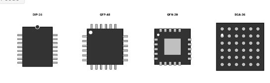
- Package Types: Throughhole > DIP (breadboard friendly), SIP (memory modules), PGA (old CPUs)
- Packgage Types: SMD > SOIC (standard small outline), QFP (Quad Flat Pack, leads on 4 sides), QFN (Quad Flat NO-Leads, just small pads under the package), BGA (Ball Grid Array, Balls underneath)
- Educational Tapeout Typical > QFN, Bare Die (on carrier boards), Chip-on-Board (wirebond directly to PCB)
Wire-Bonding Tips:
- Decide which die pad connects to which package pin
- Assign Power (VDD) and Ground (GND) pins
- Keep Power/Ground pads on OPPOSITE sides of the die from Signal pads to simplify routing and reduce noise coupling
- Define any special requirements (short wries for high-speed signals)
Evaluation Board Design: Components
- Power Supply > Clean VDD and GND
- Decoupling Capacitors > Filter out power noise
- Clock Source > Crystal or Oscillator
- Reset Circuit > Power-ON Reset
- I/O Connector > Access to chip pins
- Debug Headers > Logic analyzer, JTAG
- CMOS doesn’t like gold…charge carrier
- Scoppy + Raspberry Pi Pico 2 (WIFI) > oscilloscope on your mobile
Final Presentation Guidelines
Show - block diagram - smaller pieces of the diagram - verilog code > executes and output, test bench - map to standard cells > screen grab of KLayout
Produce for Upload presentation.png slide saved in root of website
Assignment
[x] Run Final DRC/LVS on your design [ ] Document your Chip: functionality, pin assignment, and interface details (e.g. timing parameters, frequencies, baud rates) [xx] Develop a Verification Test Plan [x] Prepare your Presentation for Thursday!
Run Final DRC/LVS on My Design
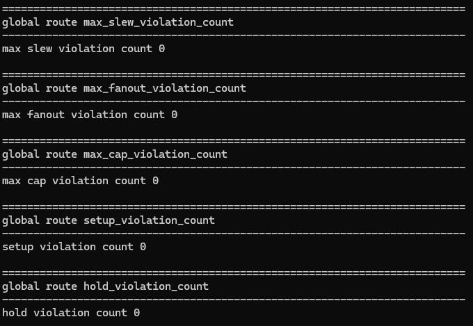
DRC ran without issue. Since the design is fully made using standard cells, there were no geometry and spacing rule violations. Here is the 5_rout_drc.rpt which is empty, indicating zero DRC violations.
‘less 5_route_drc.rpt’ command in WSL terminal to view the report
Viewing the “4_global_route.rpt” file confirms no DRC violations.
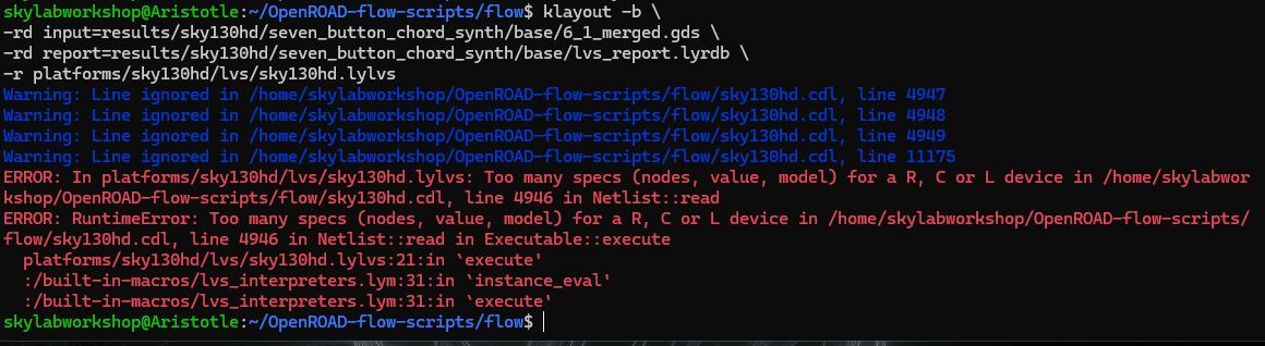
LVS was harder. With the toolchain I had, mostly a collection made available by installing OpenRoad, the .tech file needed for LVS check with Magic was missing. After debugging with ‘Chatty’ for a while, the conclusion was to go with KLayout for the LVS check.
Error in Magic
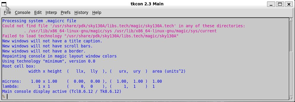
.tech File not Found

Support File Mismatch
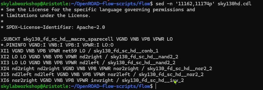
A “Failing Subcircuit
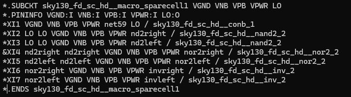
.SUBCKT sky130_fd_sc_hd__macro_sparecell1 VGND VNB VPB VPWR LO
This definition has 5 pins. But later inside CDL (circuit description language, i.e. SPICE), the same cell is being instantiated with 6 or 7 pins…causing LVS Parser to stop. ChatGPT describes this as a “quirk of the OpenRoad-flow-scripts Sky130 CDL” when used with KLayout LVS.
Some “Spare Cells Definitions” don’t parse cleanly, causing “pin count mismatch between circuit definition and circuit call”
Fortunately, the problematic cell is a “Filler Cell” and inconsequential for the functionality of the project circuit. So it can be safely removed for LVS testing.
One error managed…another one appears.
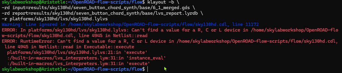
- A Passive Device Line is encountered that does not have a required value.
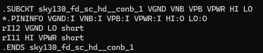
- Two resistors do not have values
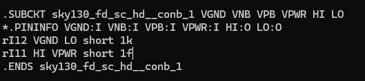
- Arbitrary values added to satisfy LVS requirements
- LVS does not concern itself with values, only connectivity
But another error appears…
At this point, ChatGPT advises that the issue is not with the chip design, but with syntax incompatibility between OpenRoad CDL, KLayout LVS and Sky130 device. To stop chasing ghosts, ChatGPT states the solution will require the installation of the full Sky130 PDK stack (a multi-gigabyte install)…then run LVS with Magic and Netgen. I am choosing not to do this right now…due to time limitations. As ChatGPT states that my design is a pure standard-cell digital logic so LVS checks should not be a problem.
Chip Functionality
My chip design emulates the functionality of a commercial synthesizer called the HiChord,
…which produces 7 diatonic chords audio output from 7 buttons. Only one button can be pressed at a time (no sound generated with multiple buttons pressed). The audio output is a 1-bit square wave.
C major > C E G
D min > D F A
E min > E G B
F major > F A C
G major > G B D
A min > A C E
B dim > B D F
- The system clock input drives note divider logic
- Internal counters divide the clock to generate square-wave frequencies (note tones) (7 notes of 7 different frequencies in total)
- 3 notes are combined into a chord and outputted as audio
- The system resets to no sound when the button is released
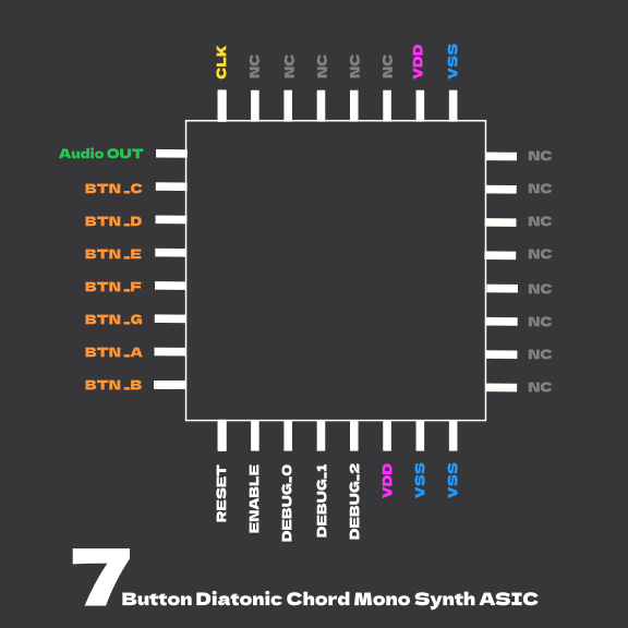
Pin Assignments
| Signal | I/O | Pin NO. | Description |
|---|---|---|---|
| Clk | INPUT | 1 | External System Clock |
| reset | INPUT | 14 | Resets counters and output state |
| Button_C | INPUT | 2 | Select C Major chord |
| Button_D | INPUT | 2 | Select D minor chord |
| Button_E | INPUT | 2 | Select E minor chord |
| Button_F | INPUT | 2 | Select F Major chord |
| Button_G | INPUT | 2 | Select G Major chord |
| Button_A | INPUT | 2 | Select A minor chord |
| Button_B | INPUT | 2 | Select B Diminished chord |
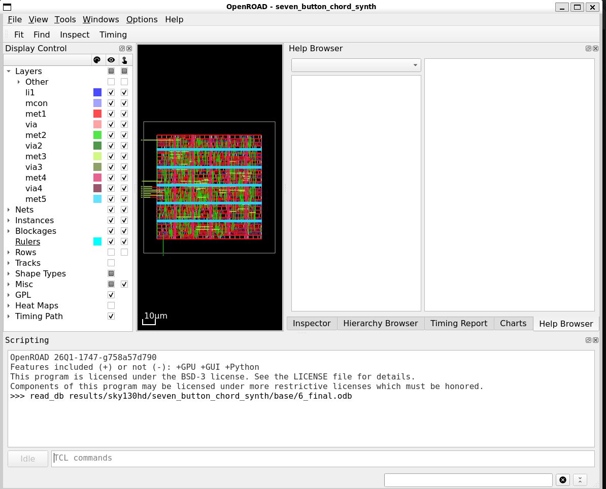
Open final circuit design in OpenRoad to determine where the pin locations are.
Open OpenRoad visualizer
/home/skylabworkshop/OpenROAD-flow-scripts/tools/install/OpenROAD/bin/openroad -gui
Open .odb file
read_db results/sky130hd/seven_button_chord_synth/base/6_final.odb
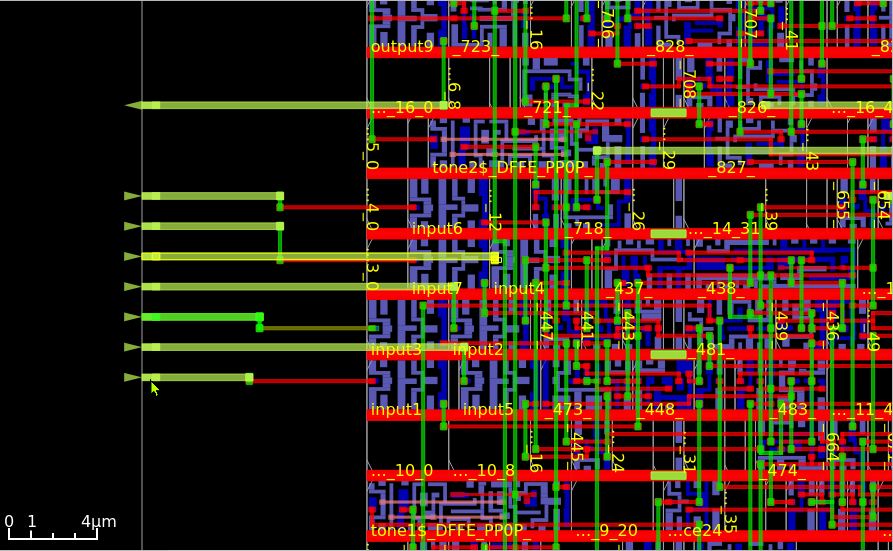
From the board image, 10 INPUT and OUTPUT paths are clearly indicated as green lines. But which is which?
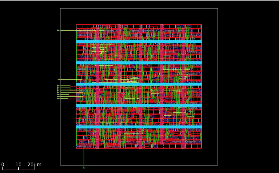
Zooming in, I can see 7 lines with arrows at the end pointing inwards and terminating into circuit blocks indicated as INPUT. These must be the connections to INPUT buttons. There is also a single line pointing outwards towards a cell called OUTPUT. This is surely the audio out line.
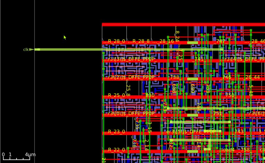
At the top left corner of the circuit design is a single line with an arrow pointing inwards and labelled ‘clk’. This is clearly the Clock line.
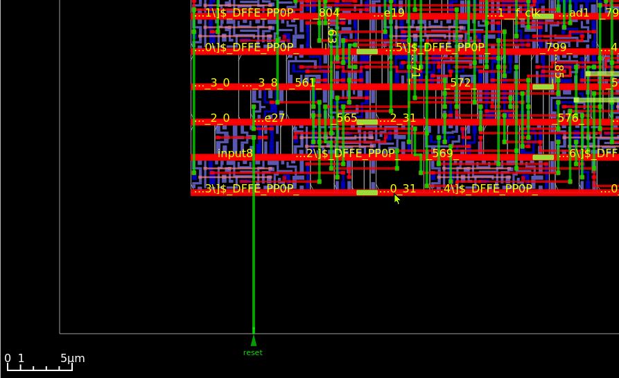
At the lower left corner of the circuit design is a single line with an arrow pointing inwards and labelled ‘reset’. This is clearly the Reset line.
With all the signal lines understood, it is time to identify the POWER lines. When a command is inputted to highlight the VDD (Power Supply, Positive Voltage) and VSS (Ground, 0V reference) lines, a green grid is overlaid on top of the signal lines.
VDD
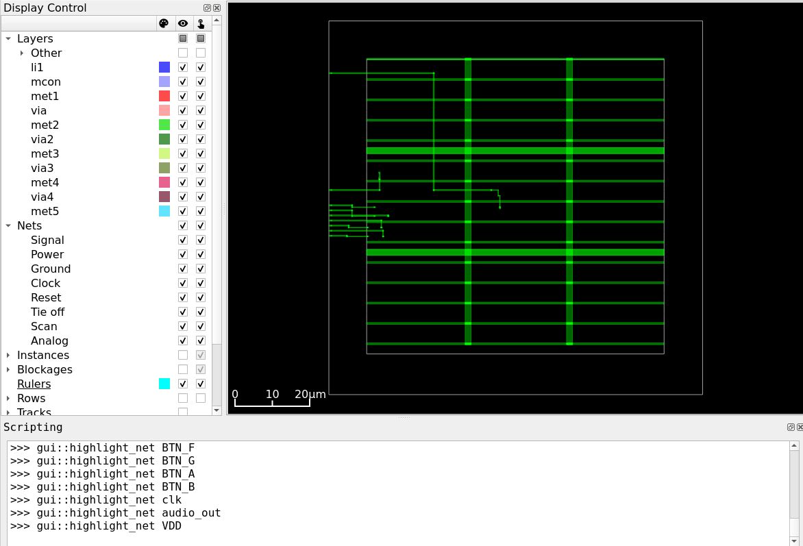
VSS
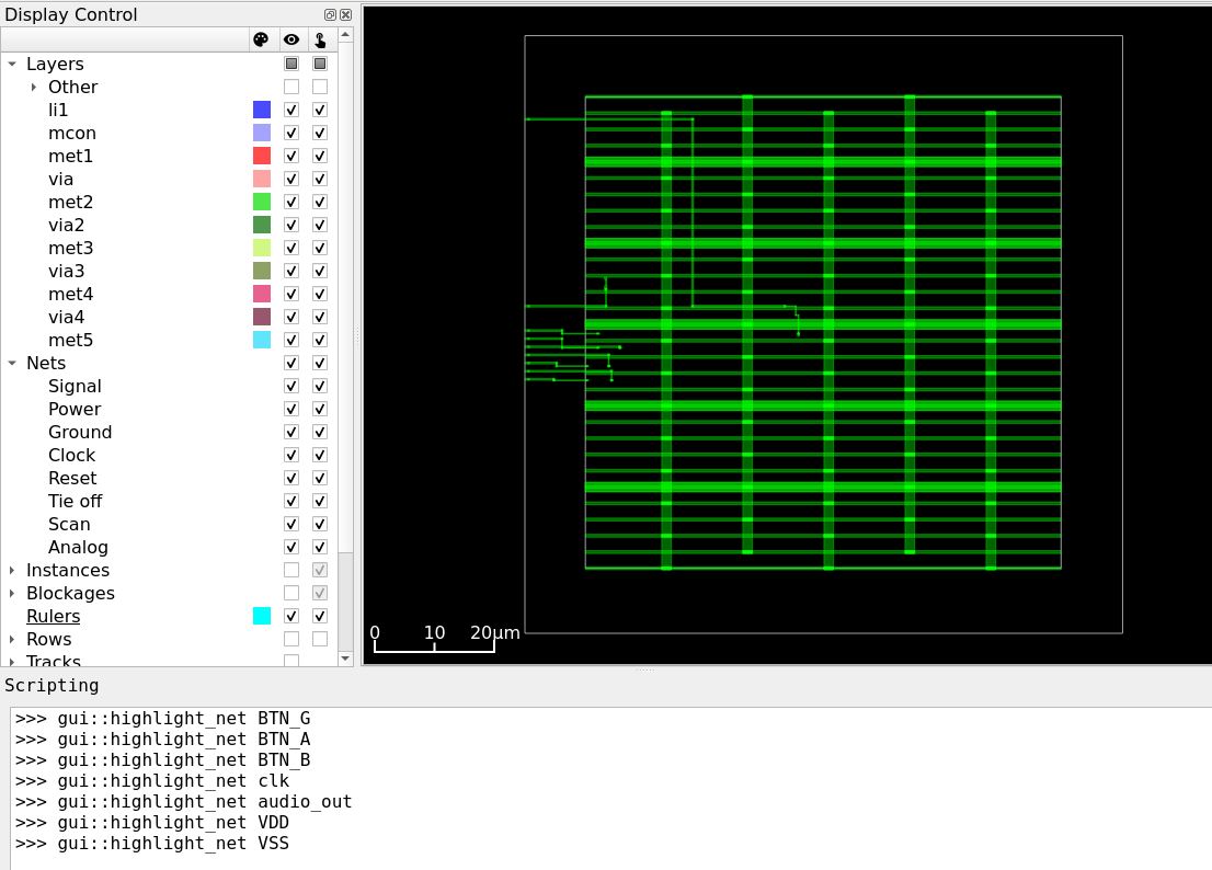
…so there are multitudes of options as to where to extend these lines to the edge of the package.
I like the 4-sided pinout layout of the Quad Flat Package (QFP) package and the ‘gull-wing’ leads that make for easier soldering, so decided to go forward with that for my chip. I learned a bit about the QFP Package from the Electrical-information website. The smallest QFP package has 32 pins.
 image from Turbosquid
This is my Pin Assignment strategy for a QFN chip package.
Interface Details
- Assuming 50MZ (FPGA) clock signal
- Active HIGH button INPUT signal
- Reset to no-sound when nothing pressed or more than one button pressed
- Output 1-bit Square Wave audio to an amplifier or speaker
Verification Test Plan
Simulation via Yosys will be conducted, confirming in GTKwave waveforms
The plan is to also test the circuit in hardware on an FPGA.
- Test Reset Behavior > confirm counter clear and no audio output
- Test No Button Press Behavior > confirm counter clear and no audio output
- Test Individual Button Press Behavior > confirm that each button generates the appropriate tone
- Test Multiple Button Press Behavior > confirm counter clear and no audio output
- Test Button Transistion Behavior > confirm clean chord switching from one button press to another
- Test Long Press Behavior > confirm that audio output remains persistent if button is held down