Session 2: Analog Basics
Summary
Electrons flow through conductors like water through pipes Passive components (R, L, C) modify current flow without amplification Transistors (NMOS, PMOS) are voltage-controlled switches CMOS logic uses complementary transistor pairs to build gates SPICE simulates circuits from text netlists Clock distribution (H-tree) ensures synchronized operation Schmitt triggers clean up noisy signals with hysteresis
Homework
- Modify the AND gate netlist to create an OR gate instead
- Hint: Swap the series/parallel arrangement of transistors
- Schmitt trigger analysis: Look up a CMOS Schmitt trigger schematic and identify which transistors set the upper vs lower threshold
- Optional: Build a simple circuit (LED + resistor + button) in TinkerCAD and observe current flow
Assignment 1 — AND gate to OR gate
I created the netlist files inside the container in /foss/designs/analog_course.
cd /foss/designs
mkdir analog_course
cd analog_course
gedit and.sp &
This is the AND gate netlist provided by our teacher. The AND gate uses two PMOS in parallel for the pull-up network, and two NMOS in series for the pull-down network:
* AND gate ngspice example

.model mosn NMOS level=49 version=3.3.0 tox=10n nch=1e17 nsub=5e16
.model mosp PMOS level=49 version=3.3.0 tox=10n nch=1e17 nsub=5e16

vsup VDD 0 1

Mp1 nOUT A VDD VDD mosp L=0.35u W=2u
Mp2 nOUT B VDD VDD mosp L=0.35u W=2u

Mn1 nOUT A npd 0 mosn L=0.35u W=2u
Mn2 npd B 0 0 mosn L=0.35u W=2u

Mp3 AND nOUT VDD VDD mosp L=0.35u W=2u
Mn3 AND nOUT 0 0 mosn L=0.35u W=2u

vin1 A 0 PWL(0 0 2mS 0 2.001mS 1V 3mS 1V 3.001mS 0)
vin2 B 0 PWL(0 0 1mS 0 1.001mS 1V 2.5mS 1V 2.5001mS 0)

.control
  tran 100n 4m
  plot v(A)
  plot v(B)
  plot v(AND)
.endc
Running the AND simulation:
ngspice and.sp
plot v(A) v(B) v(AND)
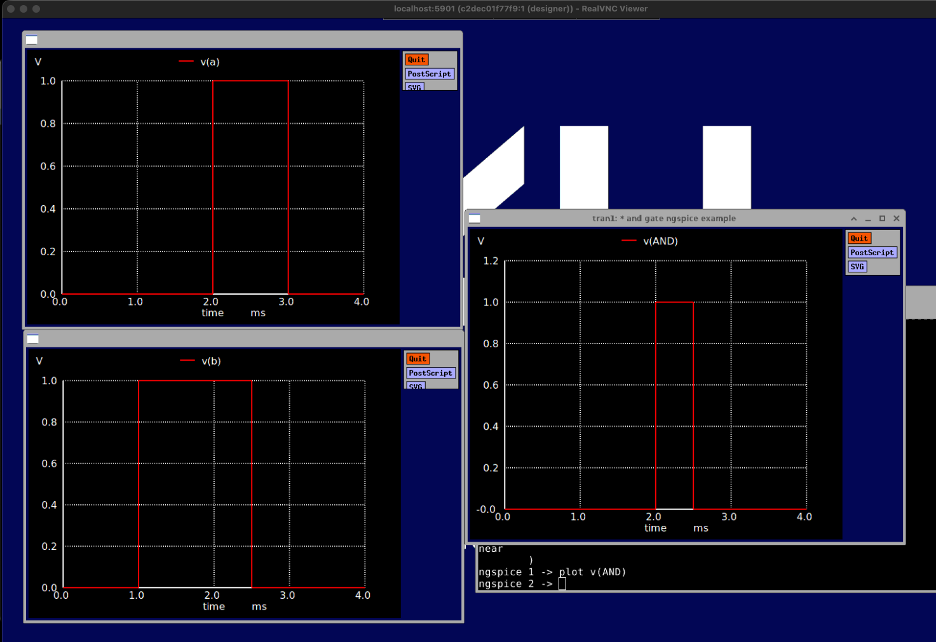
The AND output is HIGH only when both A and B are HIGH at the same time. You can see this in the waveform the output only goes to 1V during the overlap between 2ms and 2.5ms.
To convert the AND gate into an OR gate, the transistor arrangement must be swapped:
| Gate | PMOS (pull-up) | NMOS (pull-down) |
|---|---|---|
| AND | Parallel | Series |
| OR | Series | Parallel |
This is the OR gate netlist:
* OR gate ngspice example

.model mosn NMOS level=49 version=3.3.0 tox=10n nch=1e17 nsub=5e16
.model mosp PMOS level=49 version=3.3.0 tox=10n nch=1e17 nsub=5e16

* 1 V power supply
vsup VDD 0 1

* OR pull-up network -- two pmos in series
Mp1 npu A VDD VDD mosp L=0.35u W=2u
Mp2 nOUT B npu VDD mosp L=0.35u W=2u

* Pull-down network -- two nmos in parallel
Mn1 nOUT A 0 0 mosn L=0.35u W=2u
Mn2 nOUT B 0 0 mosn L=0.35u W=2u

* Inverter, or a logical NOT
Mp3 OR nOUT VDD VDD mosp L=0.35u W=2u
Mn3 OR nOUT 0 0 mosn L=0.35u W=2u

* Input voltage source
vin1 A 0 PWL(0 0 2mS 0 2.001mS 1V 3mS 1V 3.001mS 0)
vin2 B 0 PWL(0 0 1mS 0 1.001mS 1V 2.5mS 1V 2.5001mS 0)

.control
  tran 100n 4m
  plot v(A)
  plot v(B)
  plot v(OR)
.endc
ngspice or.sp
plot v(A) v(B) v(OR)
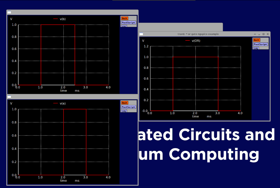
The OR output is HIGH from 1ms onwards — as soon as either A or B goes HIGH. ✅
Assignment 2 — Schmitt Trigger Analysis
A Schmitt trigger is a circuit that has two different threshold voltages for rising and falling inputs. This gap is called hysteresis and prevents noisy signals from causing multiple unwanted transitions.
gedit schmitt.sp &
* Schmitt trigger ngspice example

.model mosn NMOS level=49 version=3.3.0 tox=10n nch=1e17 nsub=5e16
.model mosp PMOS level=49 version=3.3.0 tox=10n nch=1e17 nsub=5e16

* 1 V power supply
vsup VDD 0 1

* Schmitt trigger circuit
Mp1 OUT IN VDD VDD mosp L=0.35u W=2u
Mp2 FB OUT VDD VDD mosp L=0.35u W=4u
Mn1 OUT IN nfb 0 mosn L=0.35u W=2u
Mn2 nfb 0 0 0 mosn L=0.35u W=4u

* Input: slow ramp up then down
vin IN 0 PWL(0 0 2mS 1V 4mS 0)

.control
  tran 10n 4m
  plot v(IN) v(OUT)
.endc
ngspice schmitt.sp
plot v(IN) v(OUT)
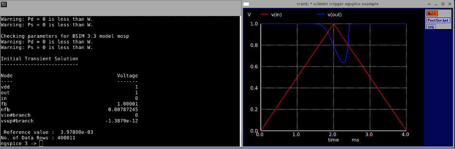
The red line shows the input voltage ramping up and down. The blue output switches at different voltages depending on the direction of the input.
| Transition | Threshold |
|---|---|
| Rising input (LOW → HIGH) | ~0.62 V |
| Falling input (HIGH → LOW) | ~0.34 V |
| Hysteresis window | ~0.28 V |
The transistors responsible for each threshold are:
| Transistor | Role |
|---|---|
| Mp2 (PMOS W=4u) | Sets the upper threshold (~0.62V) |
| Mn2 (NMOS W=4u) | Sets the lower threshold (~0.34V) |
To better understand how the Schmitt trigger rejects noise, I created a second simulation with a noisy input signal:
* Schmitt trigger with noisy signal

.model mosn NMOS level=49 version=3.3.0 tox=10n nch=1e17 nsub=5e16
.model mosp PMOS level=49 version=3.3.0 tox=10n nch=1e17 nsub=5e16

vsup VDD 0 1

Mp1 OUT IN VDD VDD mosp L=0.35u W=2u
Mp2 FB OUT VDD VDD mosp L=0.35u W=4u
Mn1 OUT IN nfb 0 mosn L=0.35u W=2u
Mn2 nfb 0 0 0 mosn L=0.35u W=4u

* Noisy signal -- rises with trembling, then falls with trembling
vin IN 0 PWL(0 0 1mS 0.3V 1.5mS 0.4V 1.6mS 0.35V 1.7mS 0.45V 1.8mS 0.4V 2mS 1V 3mS 1V 3.5mS 0.6V 3.6mS 0.65V 3.7mS 0.58V 3.8mS 0.6V 4mS 0)

.control
  tran 10n 4m
  plot v(IN) v(OUT)
.endc
ngspice schmitt2.sp
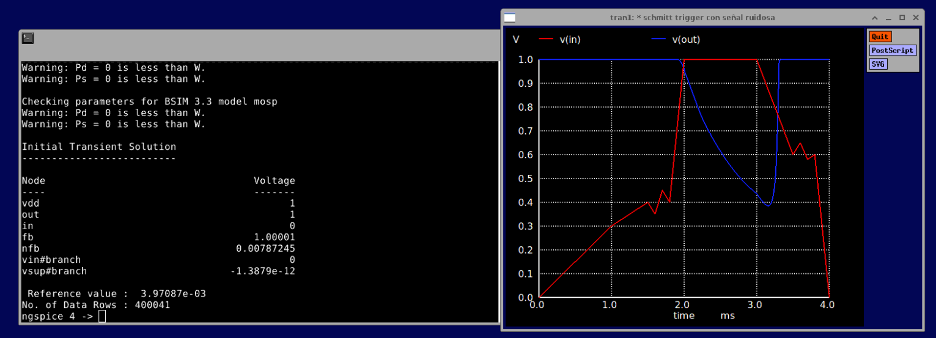
The red line trembles in the middle zone but the blue output ignores all of it and only switches cleanly when the signal crosses the thresholds. This is exactly what the Schmitt trigger is designed for.
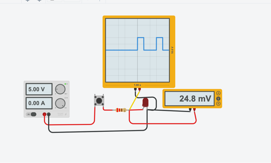
Optional — TinkerCAD
Falstad Circuit Simulator was also used to visualize circuit behavior in the browser. I tested a simple LED + resistor + button circuit and used the oscilloscope view to observe the signal waveforms.