Session 4: Layout & Fabrication
Summary
Layout → Verification (DRC/LVS) → Tape Out → Fabrication → Delivery
Homework
- Block diagram: Sketch your project’s architecture showing major modules and data flow
- Explore a standard cell: Open the sky130 standard cell library in KLayout and find an inverter (sky130_fd_sc_hd__inv_1). Identify metal, poly, and diffusion layers
- Connect the dots: Pick one block from your diagram — what standard cells might implement it?
Assignment 1 — Block Diagram
My project is the APOLLO-4G — a 4-bit CPU inspired by the Intel 4004 from 1971, the same year as the Apollo 14 mission.
The architecture consists of the following modules connected in a pipeline:
                    ┌──────────────────────────────────────┐
                    │         MINI CPU 4-bit               │
                    │                                      │
Clock ────────────► │  ┌──────────┐      ┌─────────────┐  │
Reset ────────────► │  │ Program  │─────►│   Control   │  │
                    │  │ Counter  │      │    Unit     │  │
                    │  └──────────┘      └──────┬──────┘  │
                    │        │                  │          │
                    │        ▼                  ▼          │
                    │  ┌──────────┐      ┌─────────────┐  │
                    │  │   ROM    │─────►│     ALU     │  │
                    │  │(Program) │      │ADD,SUB,AND  │  │
                    │  └──────────┘      │ OR,XOR      │  │
                    │                    └──────┬──────┘  │
                    │                           │          │
                    │                    ┌──────▼──────┐  │
                    │                    │  Register A │  │
                    │                    │  (4-bit)    │  │
                    │                    └──────┬──────┘  │
                    │                           │          │
                    │                    ┌──────▼──────┐  │
                    │                    │    Flags    │  │
                    │                    │ Zero, Carry │  │
                    │                    └──────┬──────┘  │
                    │                           │          │
                    │                    ┌──────▼──────┐  │
                    │                    │   Branch/   │  │
                    │                    │    Jump     │  │
                    │                    └──────┬──────┘  │
                    │                           │          │
                    │                    ┌──────▼──────┐  │
                    │                    │    UART     │  │
                    │                    │   Output    │  │
                    └────────────────────┴─────────────┴──┘
                                               │
                                               ▼
                                        Terminal output
The CPU supports 5 instructions: LOAD, ADD, SUB, OUT, HALT. The ROM stores the program — in the final version it computes the Fibonacci sequence.
Assignment 2 — Explore a Standard Cell in KLayout
I opened KLayout with the Sky130 standard cell library:
klayout /foss/pdks/sky130A/libs.ref/sky130_fd_sc_hd/gds/sky130_fd_sc_hd.gds
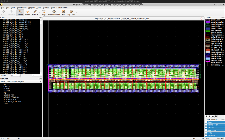
The first step was to import the correct technology file so the layers show proper names instead of numbers. I went to Tools → Manage Technologies, right-clicked, chose Import Technology, and loaded:
/foss/pdks/sky130A/libs.tech/klayout/tech/sky130A.lyt
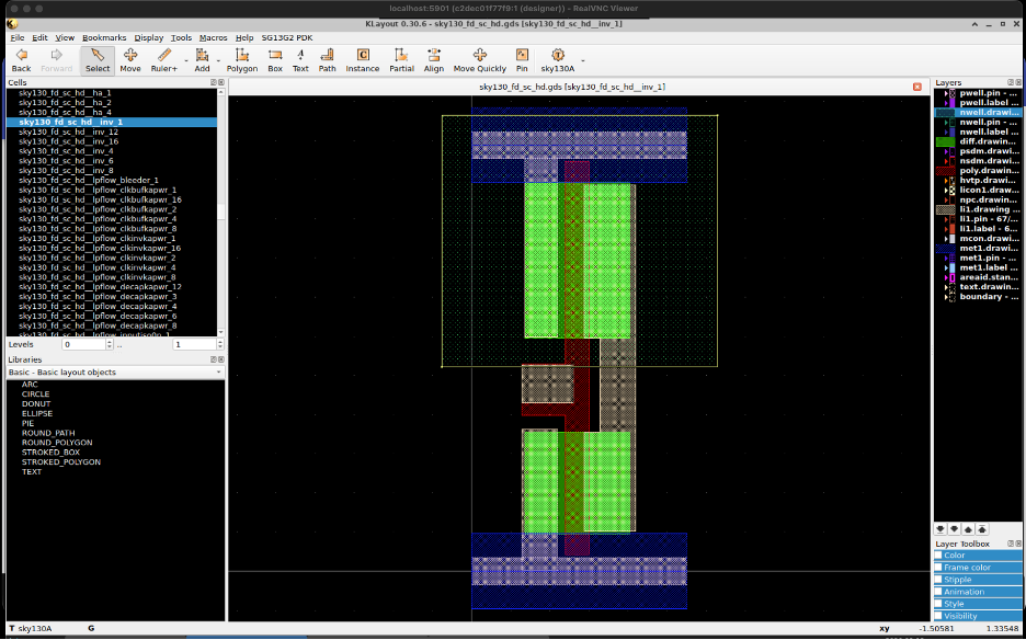
Then I found the inverter sky130_fd_sc_hd__inv_1 in the Cells panel, right-clicked and selected Show as New Top.

To clean up the view, I right-clicked on the Layers panel and selected Hide empty layers.
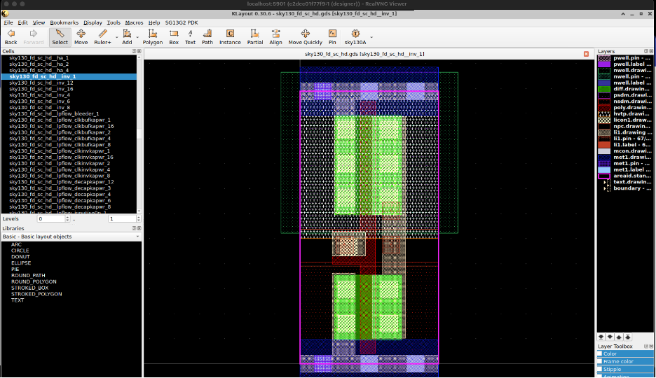
With the Sky130A technology loaded, the layers now show meaningful names:
| Layer | Color | What it is |
|---|---|---|
| nwell.drawing | Dark blue | N-well where the PMOS transistor lives |
| diff.drawing | Bright green | Diffusion — source and drain regions |
| poly.drawing | Red/brown | The gate of the transistor |
| li1.drawing | Orange/brown | Local interconnect — short connections |
| met1.drawing | Light blue | Metal 1 — main signal wires |
I also explored the dfxtp_1 flip-flop cell — this is the most important cell for my CPU project, as it stores state in the registers, program counter, and UART.
klayout /foss/pdks/sky130A/libs.ref/sky130_fd_sc_hd/gds/sky130_fd_sc_hd.gds
Search for dfxtp_1 → Show as New Top.
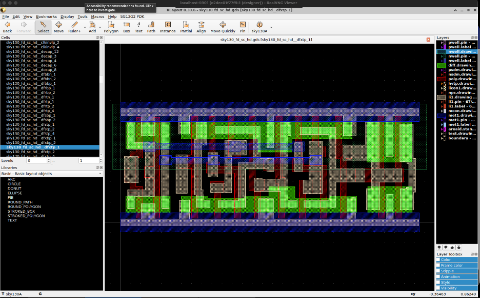
The flip-flop is much more complex than the inverter — it has around 20 transistors compared to 2, because it needs to store a bit of memory.
Assignment 3 — Connect the Dots
The question is: what standard cells does the APOLLO-4G CPU need?
| CPU Block | Standard Cells |
|---|---|
| Program Counter | sky130_fd_sc_hd__dfxtp_1 + sky130_fd_sc_hd__a21o_1 |
| ROM | sky130_fd_sc_hd__mux4_1 + sky130_fd_sc_hd__buf_1 |
| ALU | sky130_fd_sc_hd__xor2_1 + sky130_fd_sc_hd__and2_1 + sky130_fd_sc_hd__or2_1 |
| Register A | sky130_fd_sc_hd__dfxtp_1 |
| Flags Zero/Carry | sky130_fd_sc_hd__nor2_1 + sky130_fd_sc_hd__inv_1 |
| Branch/Jump | sky130_fd_sc_hd__mux2_1 |
| UART Output | sky130_fd_sc_hd__dfxtp_1 + sky130_fd_sc_hd__buf_4 |
The dfxtp_1 flip-flop is the most used cell in the entire CPU:
- Program Counter → 4 flip-flops (one per bit)
- Register A → 4 flip-flops
- Flags → 2 flip-flops (zero and carry)
- UART → 8 flip-flops
The CPU needs approximately 20-30 flip-flops in total and they all look exactly like the dfxtp_1 cell we explored in KLayout.
Tools Used
| Tool | Purpose |
|---|---|
| KLayout | IC layout viewer — inspects GDS files |
| Sky130A PDK | Technology file for layer names and colors |