Session 6: Synthesis & Physical Design
Summary
Synthesis converts RTL to gates Place & Route creates physical layout Timing analysis ensures your design meets speed requirements GDS is the final output for manufacturing
Homework
- Synthesize your design — review gate count and check for unintended latches
- Run place and route flow
- Analyze timing reports — identify and fix any violations
- Generate GDS and review layout in KLayout
Assignment 1 — Synthesize your design
Synthesis is the process of converting the Verilog RTL description into a gate-level netlist made of real standard cells from the Sky130 library. Yosys reads all the module files, checks the hierarchy, optimizes the logic, and then maps everything to specific cells like NAND gates, flip-flops, and multiplexers.
I created the synthesis script using Python to avoid typos and ensure repeatability. The script reads all 6 Verilog modules, runs the synthesis, maps to Sky130 cells using dfflibmap and abc, and writes the final netlist to synth.v:
python3 << 'PYEOF'
lines = [
    "read_verilog alu.v",
    "read_verilog debounce.v",
    "read_verilog rom.v",
    "read_verilog control_unit.v",
    "read_verilog uart_tx.v",
    "read_verilog top.v",
    "",
    "hierarchy -check -top top",
    "synth -top top",
    "",
    "dfflibmap -liberty /foss/pdks/sky130A/libs.ref/sky130_fd_sc_hd/lib/sky130_fd_sc_hd__tt_025C_1v80.lib",
    "abc -liberty /foss/pdks/sky130A/libs.ref/sky130_fd_sc_hd/lib/sky130_fd_sc_hd__tt_025C_1v80.lib",
    "",
    "clean",
    "stat",
    "",
    "write_verilog -noattr synth.v"
]
with open('/foss/designs/mini_cpu/synth.tcl', 'w') as f:
    f.write('\n'.join(lines))
print('synth.tcl creado!')
PYEOF
Running Yosys:
cd /foss/designs/mini_cpu
yosys -s synth.tcl 2>&1 | tail -60
Gate count results
/foss/designs/mini_cpu > yosys -s synth.tcl 2>&1 | grep -A 50 "=== design hierarchy ==="
=== design hierarchy ===
        +----------Count including submodules.
        |
      270 top
       99 alu
       36 control_unit
       14 rom
      110 uart_tx

      270 cells
       82   $_ANDNOT_
        2   $_AND_
        6   $_DFFE_PN0N_
       39   $_DFFE_PN0P_
        1   $_DFFE_PN1P_
        3   $_DFF_PN0_
       18   $_MUX_
       17   $_NAND_
       15   $_NOR_
       10   $_NOT_
       11   $_ORNOT_
       38   $_OR_
        8   $_XNOR_
       20   $_XOR_
        4 submodules
        1   alu
        1   control_unit
        1   rom
        1   uart_tx

8.26. Executing CHECK pass (checking for obvious problems).
Checking module control_unit...
Checking module alu...
Checking module rom...
Checking module top...
Checking module uart_tx...
Found and reported 0 problems.

9. Executing DFFLIBMAP pass (mapping DFF cells to sequential cells from liberty file).

=== design hierarchy ===
        +----------Count including submodules.
        |
      221 top
       51 alu
       32 control_unit
        8 rom
      109 uart_tx

      221 cells
        1   sky130_fd_sc_hd__a21boi_0
        2   sky130_fd_sc_hd__a21o_1
        9   sky130_fd_sc_hd__a21oi_1
        3   sky130_fd_sc_hd__a22o_1
        8   sky130_fd_sc_hd__a22oi_1
        1   sky130_fd_sc_hd__a31o_1
        6   sky130_fd_sc_hd__a31oi_1
        1   sky130_fd_sc_hd__a32o_1
        1   sky130_fd_sc_hd__a41oi_1
        1   sky130_fd_sc_hd__and2_0
        1   sky130_fd_sc_hd__and3_1
        1   sky130_fd_sc_hd__and4_1
        4   sky130_fd_sc_hd__clkinv_1
       48   sky130_fd_sc_hd__dfrtp_1
        1   sky130_fd_sc_hd__dfstp_2
        1   sky130_fd_sc_hd__lpflow_inputiso1p_1
        6   sky130_fd_sc_hd__lpflow_isobufsrc_1
        3   sky130_fd_sc_hd__maj3_1
       15   sky130_fd_sc_hd__mux2_1
       37   sky130_fd_sc_hd__nand2_1
        3   sky130_fd_sc_hd__nand2b_1
        2   sky130_fd_sc_hd__nand3_1
        1   sky130_fd_sc_hd__nand3b_1
        2   sky130_fd_sc_hd__nand4_1
       14   sky130_fd_sc_hd__nor2_1
        2   sky130_fd_sc_hd__nor3_1
        2   sky130_fd_sc_hd__nor3b_1
        3   sky130_fd_sc_hd__nor4_1
        1   sky130_fd_sc_hd__nor4b_1
221 cells total, 48 flip-flops (dfrtp_1), 0 latches, 0 problems. ✅
Yosys runs in two stages. In the first stage it uses generic internal cell types like $_ANDNOT_, $_DFF_PN0_, and $_MUX_ — these are technology-independent representations of the logic. In the second stage (dfflibmap + abc), it maps those generic cells to real Sky130 standard cells like sky130_fd_sc_hd__dfrtp_1 (a D flip-flop with reset), sky130_fd_sc_hd__nand2_1 (a 2-input NAND gate), and sky130_fd_sc_hd__mux2_1 (a 2-to-1 multiplexer). This is what makes the design physically manufacturable.
The module breakdown after mapping:
| Module | Cells | Description |
|---|---|---|
| uart_tx | 109 | Serial UART transmitter — most complex because it manages baud rate counting and shift register logic |
| alu | 51 | Arithmetic Logic Unit — ADD, SUB, AND, OR, XOR operations |
| control_unit | 32 | Instruction decoder — reads opcodes from ROM and controls the rest of the CPU |
| rom | 8 | Program memory — stores the Fibonacci sequence instructions |
| Total | 221 | Complete APOLLO-4G CPU |
The most important thing to check is latches. A latch is inferred when combinational logic has an incomplete always @(*) block for example, when an if statement has no else. Latches cause unpredictable behavior in real hardware. The Found and reported 0 problems message from Yosys confirms the RTL is clean. ✅
Assignment 2 — Place and Route
Place and Route (P&R) takes the gate-level netlist from Yosys and gives every cell a physical location on the chip, then routes the metal wires connecting them. OpenROAD performs this in stages: floorplanning (define the chip area), placement (position the cells in rows), clock tree synthesis (distribute the clock signal evenly), and routing (draw the metal connections).
I created the constraints file which tells OpenROAD about the clock speed and I/O timing requirements. The constraints.sdc defines a 50 MHz clock (20 ns period), input/output delays, and marks the reset as asynchronous:
constraints.sdc
# 50 MHz clock (20 ns period)
create_clock -name clk -period 20 [get_ports clk]

set_input_delay  -clock clk 5 [all_inputs]
set_output_delay -clock clk 5 [all_outputs]

set_false_path -from [get_ports rst_n]
set_clock_uncertainty 0.5 [get_clocks clk]
run_openroad.tcl
The OpenROAD script reads the technology files (LEF), the standard cell library (Liberty), and the synthesized netlist. It then defines a 160µm × 100µm die area (the standard “1 tile” size for this course), places the pins on the die boundary, runs global and detailed placement, synthesizes the clock tree, and finally routes all the signal wires:
set pdk_root $::env(PDK_ROOT)

read_lef $pdk_root/sky130A/libs.ref/sky130_fd_sc_hd/techlef/sky130_fd_sc_hd__nom.tlef
read_lef $pdk_root/sky130A/libs.ref/sky130_fd_sc_hd/lef/sky130_fd_sc_hd.lef
read_liberty $pdk_root/sky130A/libs.ref/sky130_fd_sc_hd/lib/sky130_fd_sc_hd__tt_025C_1v80.lib

read_verilog synth.v
link_design top
read_sdc constraints.sdc

initialize_floorplan \
  -die_area  "0 0 160 100" \
  -core_area "10 10 150 90" \
  -site unithd

make_tracks
place_pins -hor_layers met3 -ver_layers met2

global_placement
detailed_placement

clock_tree_synthesis
detailed_placement

set_routing_layers -signal li1-met5
global_route
detailed_route -verbose 0

report_design_area
report_checks -path_delay max -format full_clock_expanded
report_worst_slack -max
report_power

write_def mini_cpu.def
write_verilog mini_cpu_pnr.v
Running OpenROAD:
export PDK_ROOT=/foss/pdks
openroad run_openroad.tcl
OpenROAD ran placement, clock tree synthesis, and global route successfully:
/foss/designs/mini_cpu > cd /foss/designs/mini_cpu
export PDK_ROOT=/foss/pdks
openroad run_openroad.tcl
OpenROAD 26Q1-990-g15af3a5c0
Features included (+) or not (-): +GPU +GUI +Python
This program is licensed under the BSD-3 license. See the LICENSE file for details.
Components of this program may be licensed under more restrictive licenses which must be honored.
[INFO ODB-0227] LEF file: /foss/pdks/sky130A/libs.ref/sky130_fd_sc_hd/techlef/sky130_fd_sc_hd__nom.tlef, created 14 layers, 25 vias
[WARNING ODB-0220] WARNING (LEFPARS-2008): NOWIREEXTENSIONATPIN statement is obsolete in version 5.6 or later.
The NOWIREEXTENSIONATPIN statement will be ignored. See file /foss/pdks/sky130A/libs.ref/sky130_fd_sc_hd/lef/sky130_fd_sc_hd.lef at line 2.

[INFO ODB-0227] LEF file: /foss/pdks/sky130A/libs.ref/sky130_fd_sc_hd/lef/sky130_fd_sc_hd.lef, created 437 library cells
[WARNING STA-0441] set_input_delay relative to a clock defined on the same port/pin not allowed.
[WARNING IFP-0028] Core area lower left (10.000, 10.000) snapped to (10.120, 10.880).
[INFO IFP-0001] Added 29 rows of 304 site unithd.
[INFO IFP-0100] Die BBox:  (  0.000  0.000 ) ( 160.000 100.000 ) um
[INFO IFP-0101] Core BBox: ( 10.120 10.880 ) ( 149.960 89.760 ) um
[INFO IFP-0102] Core area:                        11030.579 um^2
[INFO IFP-0103] Total instances area:              2312.218 um^2
[INFO IFP-0104] Effective utilization:                0.210
[INFO IFP-0105] Number of instances:                    221
Found 0 macro blocks.
Using 2 tracks default min distance between IO pins.
[INFO PPL-0001] Number of available slots 484
[INFO PPL-0002] Number of I/O             11
[INFO PPL-0003] Number of I/O w/sink      10
[INFO PPL-0004] Number of I/O w/o sink    1
[INFO PPL-0005] Slots per section         200
[INFO PPL-0008] Successfully assigned pins to sections.
[INFO PPL-0012] I/O nets HPWL: 523.00 um.
[INFO GPL-0001] ---- Initialize GPL Main Data Structures
[INFO GPL-0002] DBU: 1000
[INFO GPL-0003] SiteSize: (  0.460  2.720 ) um
[INFO GPL-0004] CoreBBox: ( 10.120 10.880 ) ( 149.960 89.760 ) um
[INFO GPL-0036] Movable instances area:       2312.218 um^2
[INFO GPL-0037] Total instances area:         2312.218 um^2
[INFO GPL-0035] Pin density area adjust:       182.783 um^2
[INFO GPL-0032] ---- Initialize Region: Top-level
[INFO GPL-0006] Number of instances:               221
[INFO GPL-0007] Movable instances:                 221
[INFO GPL-0008] Fixed instances:                     0
[INFO GPL-0009] Dummy instances:                     0
[INFO GPL-0010] Number of nets:                    226
[INFO GPL-0011] Number of pins:                    839
[INFO GPL-0012] Die BBox:  (  0.000  0.000 ) ( 160.000 100.000 ) um
[INFO GPL-0013] Core BBox: ( 10.120 10.880 ) ( 149.960 89.760 ) um
[INFO GPL-0016] Core area:                   11030.579 um^2
[INFO GPL-0014] Region name: top-level.
[INFO GPL-0015] Region area:                 11030.579 um^2
[INFO GPL-0017] Fixed instances area:            0.000 um^2
[INFO GPL-0018] Movable instances area:       2495.000 um^2
[INFO GPL-0019] Utilization:                    22.619 %
[INFO GPL-0020] Standard cells area:          2495.000 um^2
[INFO GPL-0021] Large instances area:            0.000 um^2
[INFO GPL-0005] ---- Execute Conjugate Gradient Initial Placement.
[INFO GPL-0051] Source of initial instance position counters:
    Odb location = 0    Core center = 221   Region center = 0
[InitialPlace]  Iter: 1 conjugate gradient residual: 0.00000011 HPWL: 3547565
[InitialPlace]  Iter: 2 conjugate gradient residual: 0.00000010 HPWL: 2045286
[InitialPlace]  Iter: 3 conjugate gradient residual: 0.00000008 HPWL: 2044819
[InitialPlace]  Iter: 4 conjugate gradient residual: 0.00000009 HPWL: 2048116
[InitialPlace]  Iter: 5 conjugate gradient residual: 0.00000008 HPWL: 2049090
[INFO GPL-0033] ---- Initialize Nesterov Region: Top-level
[INFO GPL-0023] Placement target density:       0.7000
[INFO GPL-0024] Movable insts average area:     11.290 um^2
[INFO GPL-0025] Ideal bin area:                 16.128 um^2
[INFO GPL-0026] Ideal bin count:                   683
[INFO GPL-0027] Total bin area:              11030.579 um^2
[INFO GPL-0028] Bin count (X, Y):          16 ,     16
[INFO GPL-0029] Bin size (W * H):       8.740 *  4.930 um
[INFO GPL-0030] Number of bins:                    256
[INFO GPL-0007] ---- Execute Nesterov Global Placement.
[INFO GPL-0031] HPWL: Half-Perimeter Wirelength
Iteration | Overflow |     HPWL (um) |  HPWL(%) |   Penalty | Group
---------------------------------------------------------------
        0 |   0.9290 |  6.707380e+02 |   +0.00% |  3.11e-15 |
       10 |   0.9295 |  6.454390e+02 |   -3.77% |  5.07e-15 |
       20 |   0.9296 |  6.458000e+02 |   +0.06% |  8.25e-15 |
       30 |   0.9289 |  6.458730e+02 |   +0.01% |  1.34e-14 |
       40 |   0.9279 |  6.457900e+02 |   -0.01% |  2.19e-14 |
       50 |   0.9274 |  6.456850e+02 |   -0.02% |  3.57e-14 |
       60 |   0.9274 |  6.456450e+02 |   -0.01% |  5.81e-14 |
       70 |   0.9274 |  6.456190e+02 |   -0.00% |  9.46e-14 |
       80 |   0.9274 |  6.456690e+02 |   +0.01% |  1.54e-13 |
       90 |   0.9274 |  6.461760e+02 |   +0.08% |  2.51e-13 |
      100 |   0.9274 |  6.473230e+02 |   +0.18% |  4.09e-13 |
      110 |   0.9274 |  6.498790e+02 |   +0.39% |  6.66e-13 |
      120 |   0.9274 |  6.545240e+02 |   +0.71% |  1.09e-12 |
      130 |   0.9274 |  6.621940e+02 |   +1.17% |  1.77e-12 |
      140 |   0.9274 |  6.745750e+02 |   +1.87% |  2.88e-12 |
      150 |   0.9274 |  6.923790e+02 |   +2.64% |  4.69e-12 |
      160 |   0.9142 |  7.109710e+02 |   +2.69% |  7.64e-12 |
      170 |   0.8987 |  7.178070e+02 |   +0.96% |  1.24e-11 |
      180 |   0.8924 |  7.380960e+02 |   +2.83% |  2.03e-11 |
      190 |   0.8717 |  7.934520e+02 |   +7.50% |  3.30e-11 |
      200 |   0.8471 |  8.150410e+02 |   +2.72% |  5.38e-11 |
      210 |   0.8473 |  8.648790e+02 |   +6.11% |  8.76e-11 |
      220 |   0.8058 |  9.347750e+02 |   +8.08% |  1.43e-10 |
      230 |   0.7886 |  1.008105e+03 |   +7.84% |  2.32e-10 |
      240 |   0.7375 |  1.071503e+03 |   +6.29% |  3.79e-10 |
      250 |   0.6984 |  1.160181e+03 |   +8.28% |  6.17e-10 |
      260 |   0.6591 |  1.228221e+03 |   +5.86% |  1.00e-09 |
      270 |   0.6076 |  1.328407e+03 |   +8.16% |  1.64e-09 |
      280 |   0.5661 |  1.374151e+03 |   +3.44% |  2.67e-09 |
      290 |   0.5265 |  1.506452e+03 |   +9.63% |  4.34e-09 |
      300 |   0.4942 |  1.602485e+03 |   +6.37% |  7.07e-09 |
      310 |   0.4567 |  1.702545e+03 |   +6.24% |  1.15e-08 |
      320 |   0.4046 |  1.792681e+03 |   +5.29% |  1.88e-08 |
      330 |   0.3499 |  1.860632e+03 |   +3.79% |  3.06e-08 |
      340 |   0.3099 |  1.921332e+03 |   +3.26% |  4.55e-08 |
      350 |   0.2678 |  1.967430e+03 |   +2.40% |  6.70e-08 |
      360 |   0.2430 |  2.077880e+03 |   +5.61% |  9.87e-08 |
      370 |   0.2097 |  2.164259e+03 |   +4.16% |  1.45e-07 |
      380 |   0.1788 |  2.221801e+03 |   +2.66% |  2.14e-07 |
      390 |   0.1443 |  2.267212e+03 |   +2.04% |  3.16e-07 |
      400 |   0.1379 |  2.297650e+03 |   +1.34% |  4.65e-07 |
      410 |   0.1075 |  2.355803e+03 |   +2.53% |  6.85e-07 |
      412 |   0.0995 |  2.359437e+03 |          |  7.69e-07 |
---------------------------------------------------------------
[INFO GPL-1001] Global placement finished at iteration 412
[INFO GPL-1002] Placed Cell Area             2495.0002
[INFO GPL-1003] Available Free Area         11030.5792
[INFO GPL-1004] Minimum Feasible Density        0.2300 (cell_area / free_area)
[INFO GPL-1006]   Suggested Target Densities:
[INFO GPL-1007]     - For 90% usage of free space: 0.2513
[INFO GPL-1008]     - For 80% usage of free space: 0.2827
[INFO GPL-1009]     - For 50% usage of free space: 0.4524
[INFO GPL-1014] Final placement area: 2495.00 (+0.00%)
Placement Analysis
---------------------------------
total displacement        682.0 u
average displacement        3.1 u
max displacement            9.2 u
original HPWL            2363.7 u
legalized HPWL           3196.0 u
delta HPWL                   35 %

[WARNING CTS-0104] Clock wire resistance/capacitance values are zero.
Use set_wire_rc to set them.
[INFO CTS-0050] Root buffer is sky130_fd_sc_hd__clkbuf_1.
[INFO CTS-0051] Sink buffer is sky130_fd_sc_hd__clkbuf_1.
[INFO CTS-0052] The following clock buffers will be used for CTS:
                    sky130_fd_sc_hd__clkbuf_1
[INFO CTS-0049] Characterization buffer is sky130_fd_sc_hd__clkbuf_1.
[INFO CTS-0007] Net "clk" found for clock "clk".
[INFO CTS-0010]  Clock net "clk" has 49 sinks.
[INFO CTS-0008] TritonCTS found 1 clock nets.
[INFO CTS-0097] Characterization used 1 buffer(s) types.
[INFO CTS-0201] 0 blockages from hard placement blockages and placed macros will be used.
[INFO CTS-0027] Generating H-Tree topology for net clk.
[INFO CTS-0028]  Total number of sinks: 49.
[INFO CTS-0030]  Number of static layers: 0.
[INFO CTS-0020]  Wire segment unit: 13600  dbu (13 um).
[INFO CTS-0023]  Original sink region: [(25565, 55700), (121245, 88340)].
[INFO CTS-0024]  Normalized sink region: [(1.87978, 4.09559), (8.91507, 6.49559)].
[INFO CTS-0025]     Width:  7.0353.
[INFO CTS-0026]     Height: 2.4000.
 Level 1
    Direction: Horizontal
    Sinks per sub-region: 25
    Sub-region size: 3.5176 X 2.4000
[INFO CTS-0034]     Segment length (rounded): 2.
 Level 2
    Direction: Vertical
    Sinks per sub-region: 13
    Sub-region size: 3.5176 X 1.2000
[INFO CTS-0034]     Segment length (rounded): 1.
[INFO CTS-0032]  Stop criterion found. Max number of sinks is 15.
[INFO CTS-0035]  Number of sinks covered: 49.
[INFO CTS-0018]     Created 5 clock buffers.
[INFO CTS-0012]     Minimum number of buffers in the clock path: 2.
[INFO CTS-0013]     Maximum number of buffers in the clock path: 2.
[INFO CTS-0015]     Created 5 clock nets.
[INFO CTS-0016]     Fanout distribution for the current clock = 10:2, 13:1, 16:1..
[INFO CTS-0017]     Max level of the clock tree: 2.
[INFO CTS-0098] Clock net "clk"
[INFO CTS-0099]  Sinks 52
[INFO CTS-0100]  Leaf buffers 0
[INFO CTS-0101]  Average sink wire length 84.08 um
[INFO CTS-0102]  Path depth 2 - 2
[INFO CTS-0207]  Dummy loads inserted 3
Placement Analysis
---------------------------------
total displacement         27.0 u
average displacement        0.1 u
max displacement            5.3 u
original HPWL            3414.0 u
legalized HPWL           3421.9 u
delta HPWL                    0 %

Design area 2354 um^2 21% utilization.
Startpoint: u_uart/_166_ (rising edge-triggered flip-flop clocked by clk)
Endpoint: tx (output port clocked by clk)
Path Group: clk
Path Type: max

  Delay    Time   Description
---------------------------------------------------------
   0.00    0.00   clock clk (rise edge)
   0.00    0.00   clock source latency
   0.00    0.00 ^ clk (in)
   0.19    0.19 ^ clkbuf_0_clk/X (sky130_fd_sc_hd__clkbuf_1)
   0.43    0.62 ^ clkbuf_2_3__f_clk/X (sky130_fd_sc_hd__clkbuf_1)
   0.00    0.62 ^ u_uart/_166_/CLK (sky130_fd_sc_hd__dfstp_2)
   0.64    1.26 ^ u_uart/_166_/Q (sky130_fd_sc_hd__dfstp_2)
   0.00    1.26 ^ tx (out)
           1.26   data arrival time

  20.00   20.00   clock clk (rise edge)
   0.00   20.00   clock network delay (propagated)
  -0.50   19.50   clock uncertainty
   0.00   19.50   clock reconvergence pessimism
  -5.00   14.50   output external delay
          14.50   data required time
---------------------------------------------------------
          14.50   data required time
          -1.26   data arrival time
---------------------------------------------------------
          13.24   slack (MET)


worst slack max 13.24
Group                  Internal  Switching    Leakage      Total
                          Power      Power      Power      Power (Watts)
----------------------------------------------------------------
Sequential             1.03e-04   2.98e-06   5.77e-10   1.06e-04  69.6%
Combinational          5.12e-06   5.08e-06   4.04e-10   1.02e-05   6.7%
Clock                  6.62e-06   2.94e-05   1.81e-11   3.60e-05  23.7%
Macro                  0.00e+00   0.00e+00   0.00e+00   0.00e+00   0.0%
Pad                    0.00e+00   0.00e+00   0.00e+00   0.00e+00   0.0%
----------------------------------------------------------------
Total                  1.15e-04   3.74e-05   9.98e-10   1.52e-04 100.0%
                          75.4%      24.6%       0.0%
However, during development I ran into several errors:
Error 1 — Unroutable power nets:
[ERROR DRT-0305] Net one_ of signal type POWER is not routable by TritonRoute.
This was caused by lpflow_inputiso1p_1 cells generated during synthesis. I tried multiple approaches to fix this including techmap replacements and suppressing the cells in ABC.
Error 2 — Unplaced top-level ports:
[ERROR GPL-0326] carrier_in[0] toplevel port is not placed.
Fixed by adding place_pins -hor_layers met3 -ver_layers met2 before global_placement.
Error 3 — Invalid command find_net:
Error: run_openroad.tcl, 32 invalid command name "find_net"
Fixed by removing that command entirely.
After all fixes, OpenROAD completed the global route and reported timing but detailed_route still failed because of the lpflow power cells that TritonRoute cannot handle without a proper PDN. The DEF was generated but without complete routing:
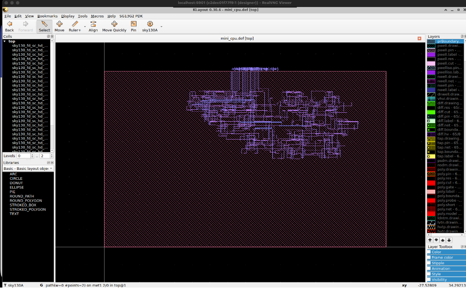
The layout in KLayout showed the placement without complete metal routing. I also ran into a KLayout error when it loaded the wrong technology:
Read error on file: /foss/pdks/ihp-sg13g2/libs.tech/klayout/tech (errno=21)
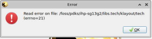
Fixed by explicitly passing the Sky130A technology file with -nn.
Step 2 — LibreLane (complete flow)
LibreLane is a wrapper around OpenROAD that automates the entire ASIC flow including power network generation (PDN), which was the root cause of the lpflow routing errors in OpenROAD. It also runs DRC, LVS, and antenna checks automatically at the end. This is why the industry uses wrappers like LibreLane or OpenLane instead of calling OpenROAD directly.
To get a proper complete GDS I switched to LibreLane:
python3 << 'PYEOF'
import json
config = {
    "DESIGN_NAME": "top",
    "VERILOG_FILES": [
        "/foss/designs/mini_cpu/alu.v",
        "/foss/designs/mini_cpu/debounce.v",
        "/foss/designs/mini_cpu/rom.v",
        "/foss/designs/mini_cpu/control_unit.v",
        "/foss/designs/mini_cpu/uart_tx.v",
        "/foss/designs/mini_cpu/top.v"
    ],
    "CLOCK_PORT": "clk",
    "CLOCK_PERIOD": 20.0,
    "PDK": "sky130A",
    "STD_CELL_LIBRARY": "sky130_fd_sc_hd"
}
with open('/foss/designs/mini_cpu/config.json', 'w') as f:
    json.dump(config, f, indent=4)
print('config.json creado!')
PYEOF
cd /foss/designs/mini_cpu
librelane config.json
LibreLane ran all 78 steps automatically:
Check for Routing DRC errors    clear ✅
Check for Magic DRC errors      clear ✅
Check for KLayout DRC errors    clear ✅
Check for LVS errors            clear ✅
Flow complete.
Assignment 3 — Timing Analysis
Static Timing Analysis (STA) checks whether signals can travel through the combinational logic fast enough to be captured by the next flip-flop before the next clock edge. The key metric is slack the difference between when a signal arrives and when it is required. Positive slack means the design meets timing; negative slack means there is a violation.
OpenROAD traces the critical path the longest path through the combinational logic and reports the slack for that path. In the APOLLO-4G, the critical path goes through the ALU (the adder chain through several maj3_1 majority gates), which makes sense since addition requires carry propagation across all 4 bits.
After P&R completed, OpenROAD reported:
Design area 2082 um^2 19% utilization.

Startpoint: b[0] (input port clocked by clk)
Endpoint: _38_ (rising edge-triggered flip-flop clocked by clk)

  Delay    Time   Description
---------------------------------------------------------
   0.00    0.00   clock clk (rise edge)
   5.00    5.00 ^ input external delay
   0.05    5.05 v u_alu/_56_/Y (nand2_1)
   0.17    5.21 v u_alu/_57_/X (xor2_1)
   0.39    5.60 v u_alu/_68_/X (maj3_1)
   0.37    6.36 v u_alu/_92_/X (maj3_1)
   0.15    6.51 ^ u_alu/_94_/Y (a21oi_1)
   0.14    6.65 ^ u_alu/_95_/X (o21a_1)
   0.00    6.65 ^ _38_/D (dfrtp_1)
           6.65   data arrival time

  20.00   20.00   clock clk (rise edge)
  -0.50   19.50   clock uncertainty
  -0.01   19.49   library setup time
          19.49   data required time
---------------------------------------------------------
          13.37   slack (MET)

worst slack max 13.37
| Metric | Value |
|---|---|
| Design area | 2082 µm² |
| Core utilization | 19% |
| Worst slack | 13.37 ns (MET) ✅ |
| Clock | 50 MHz (20 ns period) |
The slack is 13.37 ns MET the design meets timing with a very comfortable margin. This means the clock could theoretically run much faster before any violation appears. ✅
Power analysis
Power in a digital chip comes from three sources: internal switching (gates charging and discharging), net switching (wires), and static leakage. The power report shows:
Group          Internal   Switching   Leakage     Total (W)    Share
Sequential     9.06e-05   1.41e-06   5.74e-10    9.20e-05     62.4%
Combinational  4.01e-06   4.62e-06   3.26e-10    8.63e-06      5.9%
Clock          2.19e-05   2.49e-05   3.11e-11    4.68e-05     31.7%
Total          1.16e-04   3.09e-05   9.31e-10    1.47e-04    100.0%
Total power: 0.147 mW for comparison, a single LED consumes ~60 mW. The APOLLO-4G uses less than 1/400th of the power of one LED. 🔋
Assignment 4 — Generate GDS and review in KLayout
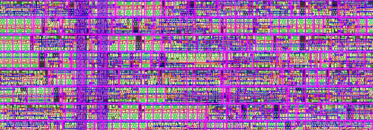
GDS (GDSII) is the final file format used for chip fabrication. It contains all the geometric shapes, metal layers, vias, and polygons that represent the physical layout of every transistor and wire in the design. When you submit a chip to a foundry, you submit the GDS file.
After LibreLane completed, I opened the final GDS with the Sky130A technology loaded so the layers show their correct names and colors:
klayout -nn /foss/pdks/sky130A/libs.tech/klayout/tech/sky130A.lyt \
  /foss/designs/mini_cpu/runs/RUN_2026-03-19_02-04-54/final/gds/top.gds &
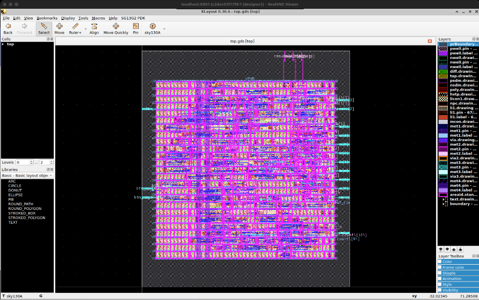
The layout shows the complete APOLLO-4G chip with all standard cells placed and fully routed across multiple metal layers. You can clearly see the I/O pins on the borders (result, btn_run, halt, clk).
Tools Used
| Tool | Purpose |
|---|---|
| Yosys | Logic synthesis — RTL to gate-level netlist |
| OpenROAD | Place and route — physical implementation |
| LibreLane | Full ASIC flow with DRC/LVS/GDS |
| KLayout | View and inspect the final GDS layout |