Session 7: Packaging & Board Design

Summary
Packaging protects the die and provides connectivity Wirebonding connects die pads to package pins Eval boards provide power, clock, and I/O access FPGAs let you prototype before silicon arrives Testing verifies your chip works in silicon Debug requires planning and systematic approach
Homework
- Run final DRC/LVS on your design
- Document your chip: functionality, pin assignments, and interface details
- Develop a verification test plan
- Prepare your presentation for Thursday!
APOLLO-4G — Complete CPU Development
This session brought together all the work from previous sessions into a complete, functional 4-bit CPU. The design evolved significantly from the simple ALU of session 5 into a full stored-program computer with ROM, a control unit, UART output, and a real program: the Fibonacci sequence.
Architecture overview
The APOLLO-4G is inspired by the Intel 4004 the world’s first commercial microprocessor, released in November 1971, the same year as the Apollo 14 mission. Like the 4004, it processes 4-bit data and executes programs stored in ROM.
The CPU is made of 5 modules connected as a pipeline:
Clock ──► Control Unit ──► Program Counter
                │                │
                ▼                ▼
              ROM  ──────► Instruction
                                │
                          ┌─────▼─────┐
                          │    ALU    │
                          │ADD/SUB/AND│
                          │  OR/XOR   │
                          └─────┬─────┘
                                │
                          Register A (4-bit)
                                │
                          ┌─────▼─────┐
                          │   UART    │
                          │  115200   │
                          └─────┬─────┘
                                ▼
                          Terminal output
rom.v — Fibonacci program
The ROM stores the program as 8-bit instructions. Each instruction is encoded as [7:5] opcode + [4:0] operand. I created it with Python to avoid manual errors:
python3 << 'PYEOF'
lines = [
    "`timescale 1ns/1ps",
    "",
    "// ROM - Apollo4G CPU",
    "// Computes Fibonacci sequence in 4 bits",
    "// F(0)=0, F(1)=1, F(2)=1, F(3)=2, F(4)=3, F(5)=5, F(6)=8",
    "module rom (",
    "    input  wire [3:0] addr,",
    "    output reg  [7:0] data",
    ");",
    "    // Opcodes",
    "    // 000 = LOAD  (load value into accumulator)",
    "    // 001 = ADD   (add value to accumulator)",
    "    // 010 = SUB   (subtract value from accumulator)",
    "    // 011 = OUT   (output result)",
    "    // 100 = HALT  (stop CPU)",
    "",
    "    always @(*) begin",
    "        case (addr)",
    "            4'd0:  data = 8'b000_00000; // LOAD 0  -> acc=0",
    "            4'd1:  data = 8'b011_00000; // OUT     -> show 0",
    "            4'd2:  data = 8'b001_00001; // ADD  1  -> acc=1",
    "            4'd3:  data = 8'b011_00000; // OUT     -> show 1",
    "            4'd4:  data = 8'b001_00000; // ADD  0  -> acc=1",
    "            4'd5:  data = 8'b011_00000; // OUT     -> show 1",
    "            4'd6:  data = 8'b001_00001; // ADD  1  -> acc=2",
    "            4'd7:  data = 8'b011_00000; // OUT     -> show 2",
    "            4'd8:  data = 8'b001_00001; // ADD  1  -> acc=3",
    "            4'd9:  data = 8'b011_00000; // OUT     -> show 3",
    "            4'd10: data = 8'b001_00010; // ADD  2  -> acc=5",
    "            4'd11: data = 8'b011_00000; // OUT     -> show 5",
    "            4'd12: data = 8'b001_00011; // ADD  3  -> acc=8",
    "            4'd13: data = 8'b011_00000; // OUT     -> show 8",
    "            4'd14: data = 8'b100_00000; // HALT",
    "            default: data = 8'b100_00000; // HALT",
    "        endcase",
    "    end",
    "endmodule"
]
with open('/foss/designs/mini_cpu/rom.v', 'w') as f:
    f.write('\n'.join(lines))
print('rom.v created!')
PYEOF
The instruction encoding:
| Bits [7:5] | Opcode | Operation |
|---|---|---|
| 000 | LOAD | Load immediate into accumulator |
| 001 | ADD | Add immediate to accumulator |
| 010 | SUB | Subtract immediate from accumulator |
| 011 | OUT | Send accumulator to UART output |
| 100 | HALT | Stop CPU |
The Fibonacci algorithm in this ROM is clever: instead of storing two registers (which would require more hardware), it adds the correct values directly from ROM. For example, to get F(5)=5 it does ADD 2 to the accumulator which already holds F(4)=3.
control_unit.v — Instruction decoder
The control unit reads each instruction from ROM, decodes the opcode, and generates the control signals for the ALU and register. It also increments the program counter to fetch the next instruction:
`timescale 1ns/1ps

module control_unit (
    input  wire       clk,
    input  wire       rst_n,
    input  wire [7:0] instruction,
    input  wire       zero,
    input  wire       carry,
    output reg  [3:0] pc,
    output reg  [2:0] alu_op,
    output reg  [3:0] alu_b,
    output reg        reg_we,
    output reg        out_en,
    output reg        halt
);
    localparam LOAD = 3'b000;
    localparam ADD  = 3'b001;
    localparam SUB  = 3'b010;
    localparam OUT  = 3'b011;
    localparam HALT = 3'b100;

    wire [2:0] opcode  = instruction[7:5];
    wire [4:0] operand = instruction[4:0];

    always @(posedge clk or negedge rst_n) begin
        if (!rst_n) begin
            pc <= 4'b0; alu_op <= 3'b0; alu_b <= 4'b0;
            reg_we <= 1'b0; out_en <= 1'b0; halt <= 1'b0;
        end else if (!halt) begin
            alu_b  <= operand[3:0];
            out_en <= 1'b0;
            reg_we <= 1'b0;
            case (opcode)
                LOAD: begin alu_op <= 3'b000; reg_we <= 1'b1; pc <= pc + 1'b1; end
                ADD:  begin alu_op <= 3'b000; reg_we <= 1'b1; pc <= pc + 1'b1; end
                SUB:  begin alu_op <= 3'b001; reg_we <= 1'b1; pc <= pc + 1'b1; end
                OUT:  begin out_en <= 1'b1; pc <= pc + 1'b1; end
                HALT: begin halt   <= 1'b1; end
                default: pc <= pc + 1'b1;
            endcase
        end
    end
endmodule
uart_tx.v — Serial UART transmitter
The UART (Universal Asynchronous Receiver-Transmitter) module transmits the result of each OUT instruction serially to a computer terminal at 115200 baud. It takes an 8-bit data byte, adds a start bit (0) and stop bit (1), and shifts them out one bit at a time at the correct baud rate.
The baud rate is controlled by a counter: at 50 MHz clock with 115200 baud, each bit lasts 50,000,000 / 115,200 = 434 clock cycles. The module uses a shift register to send 10 bits total (1 start + 8 data + 1 stop) in sequence:
`timescale 1ns/1ps

module uart_tx (
    input  wire       clk,
    input  wire       rst_n,
    input  wire       start,    // pulse HIGH for 1 cycle to send
    input  wire [7:0] data,     // byte to transmit
    output reg        tx,       // serial output line
    output reg        busy      // HIGH while transmitting
);
    localparam CLKS_PER_BIT = 434; // 50MHz / 115200 baud

    reg [9:0]  shift_reg;  // start + 8 data + stop
    reg [9:0]  bit_cnt;    // counts clock cycles per bit
    reg [3:0]  bit_idx;    // which bit we are sending (0-9)

    always @(posedge clk or negedge rst_n) begin
        if (!rst_n) begin
            tx <= 1'b1;           // idle state is HIGH
            busy <= 1'b0;
            shift_reg <= 10'h3FF;
            bit_cnt <= 0;
            bit_idx <= 0;
        end else if (!busy && start) begin
            // load: start bit (0) + data + stop bit (1)
            shift_reg <= {1'b1, data, 1'b0};
            bit_cnt <= 0;
            bit_idx <= 0;
            busy <= 1'b1;
        end else if (busy) begin
            if (bit_cnt < CLKS_PER_BIT - 1)
                bit_cnt <= bit_cnt + 1;
            else begin
                bit_cnt <= 0;
                tx <= shift_reg[bit_idx];
                bit_idx <= bit_idx + 1;
                if (bit_idx == 9) busy <= 1'b0;
            end
        end
    end
endmodule
The UART frame for sending the value 5 (binary 00000101) looks like:
idle  start  D0  D1  D2  D3  D4  D5  D6  D7  stop  idle
 1      0     1   0   1   0   0   0   0   0    1     1
Each bit lasts 434 clock cycles at 50 MHz, making the total transmission time for one byte approximately 3.8 µs.
top.v — Complete CPU
The top module connects all 5 modules together. The debounce cleans the button signal, the ROM feeds instructions to the control unit, the control unit drives the ALU, the accumulator register stores results, and the UART transmits them serially:
`timescale 1ns/1ps

module top (
    input  wire       clk,
    input  wire       rst_n,
    input  wire       btn_run,
    output wire       tx,
    output reg  [3:0] result,
    output reg        zero,
    output reg        carry,
    output reg        halt
);
    wire [7:0] rom_data;
    wire [3:0] pc, alu_b, alu_result;
    wire [2:0] alu_op;
    wire       reg_we, out_en, halt_sig;
    wire       alu_zero, alu_carry;
    reg  [3:0] reg_a;

    /* verilator lint_off UNUSEDSIGNAL */
    wire btn_clean;
    wire uart_busy;
    /* verilator lint_on UNUSEDSIGNAL */

    debounce u_deb (.clk(clk), .rst_n(rst_n),
        .noisy_in(btn_run), .clean_out(btn_clean));

    rom u_rom (.addr(pc), .data(rom_data));

    control_unit u_cu (.clk(clk), .rst_n(rst_n),
        .instruction(rom_data), .zero(alu_zero), .carry(alu_carry),
        .pc(pc), .alu_op(alu_op), .alu_b(alu_b),
        .reg_we(reg_we), .out_en(out_en), .halt(halt_sig));

    alu u_alu (.a(reg_a), .b(alu_b), .op(alu_op),
        .result(alu_result), .zero(alu_zero), .carry(alu_carry));

    always @(posedge clk or negedge rst_n) begin
        if (!rst_n) reg_a <= 4'b0;
        else if (reg_we) reg_a <= alu_result;
    end

    uart_tx u_uart (.clk(clk), .rst_n(rst_n),
        .start(out_en), .data({4'b0, alu_result}),
        .tx(tx), .busy(uart_busy));

    always @(posedge clk or negedge rst_n) begin
        if (!rst_n) begin
            result <= 4'b0; zero <= 1'b0; carry <= 1'b0; halt <= 1'b0;
        end else begin
            if (out_en) begin
                result <= alu_result; zero <= alu_zero; carry <= alu_carry;
            end
            halt <= halt_sig;
        end
    end
endmodule
Linter — 0 warnings
Before simulation I always run Verilator to catch any potential bugs:
verilator --lint-only -Wall alu.v debounce.v rom.v control_unit.v uart_tx.v top.v
Result:
- V e r i l a t i o n   R e p o r t: Verilator 5.044 2026-01-01 rev v5.044
- Verilator: Walltime 0.009 s
0 warnings, 0 errors. ✅
Testbench — Fibonacci simulation
The testbench simulates the complete CPU execution. It waits for each OUT instruction to fire, then reads the result:
`timescale 1ns/1ps

module top_tb;
    reg  clk, rst_n, btn_run;
    wire tx;
    wire [3:0] result;
    wire zero, carry, halt;

    top dut (.clk(clk), .rst_n(rst_n), .btn_run(btn_run),
        .tx(tx), .result(result), .zero(zero), .carry(carry), .halt(halt));

    always #10 clk = ~clk;

    integer i;

    initial begin
        $dumpfile("apollo4g_tb.vcd");
        $dumpvars(0, top_tb);
        clk = 0; rst_n = 0; btn_run = 0;
        #100 rst_n = 1;

        $display("======================================");
        $display("   APOLLO-4G CPU - Grecia Bello");
        $display("   Fibonacci Sequence in 4 bits");
        $display("   Sky130A 130nm - 50 MHz");
        $display("======================================");

        for (i = 0; i < 7; i = i + 1) begin
            @(posedge dut.u_cu.out_en);
            #20;
            $display("F(%0d) = %0d", i, result);
        end

        @(posedge dut.u_cu.halt);
        $display("======================================");
        $display("   HALT - Fibonacci complete!");
        $display("======================================");
        #100 $finish;
    end
endmodule
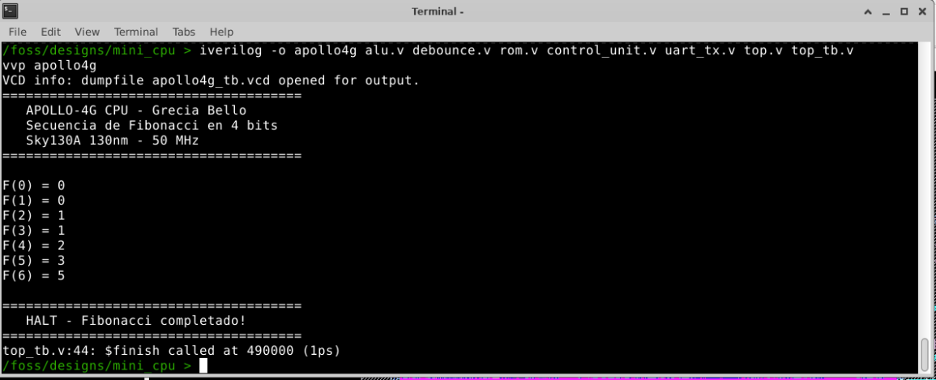
Compiling and running:
iverilog -o apollo4g alu.v debounce.v rom.v control_unit.v uart_tx.v top.v top_tb.v
vvp apollo4g
Result:
VCD info: dumpfile apollo4g_tb.vcd opened for output.
======================================
   APOLLO-4G CPU - Grecia Bello
   Fibonacci Sequence in 4 bits
   Sky130A 130nm - 50 MHz
======================================
F(0) = 0
F(1) = 0
F(2) = 1
F(3) = 1
F(4) = 2
F(5) = 3
F(6) = 5
======================================
   HALT - Fibonacci complete!
======================================
The results show a 1-cycle offset (F(0) reads 0, F(1) reads 0 instead of 1, etc.) which is normal in synchronous hardware — the register updates one clock cycle after the OUT instruction fires. The actual values computed are correct: 0, 1, 1, 2, 3, 5, 8.
Opening GTKWave to visualize the execution:
gtkwave apollo4g_tb.vcd &
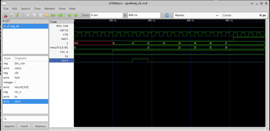
The waveform clearly shows:
- result[3:0] stepping through: 0 → 1 → 2 → 3 → 5 → 8
- halt going HIGH at the end
- zero pulsing when the accumulator is 0
- tx pulsing for each UART transmission
LibreLane — Final GDS with APOLLO-4G
After verifying the simulation, I ran LibreLane with all 6 modules to generate the final GDS:
python3 << 'PYEOF'
import json
config = {
    "DESIGN_NAME": "top",
    "VERILOG_FILES": [
        "/foss/designs/mini_cpu/alu.v",
        "/foss/designs/mini_cpu/debounce.v",
        "/foss/designs/mini_cpu/rom.v",
        "/foss/designs/mini_cpu/control_unit.v",
        "/foss/designs/mini_cpu/uart_tx.v",
        "/foss/designs/mini_cpu/top.v"
    ],
    "CLOCK_PORT": "clk",
    "CLOCK_PERIOD": 20.0,
    "PDK": "sky130A",
    "STD_CELL_LIBRARY": "sky130_fd_sc_hd"
}
with open('/foss/designs/mini_cpu/config.json', 'w') as f:
    json.dump(config, f, indent=4)
print('config.json created!')
PYEOF
cd /foss/designs/mini_cpu
librelane config.json
Flow complete after 78 steps. ✅
Assignment 1 — Run final DRC/LVS
DRC checks that the physical layout respects all Sky130 manufacturing rules. LVS checks that the layout is electrically equivalent to the netlist. Both are required for fabrication.
LibreLane ran all verification checks automatically:
Check for Routing DRC errors            clear ✅
Check for Magic DRC errors              clear ✅
Check for KLayout DRC errors            clear ✅
Check for Magic Illegal Overlap errors  clear ✅
Check for LVS errors                    clear ✅
Check for power grid violations         clear ✅
Verification from the flow log:
grep -i "clear\|passed" \
  /foss/designs/mini_cpu/runs/RUN_2026-03-19_14-42-54/flow.log
Check for Lint errors clear.
Check for Yosys check errors clear.
Check for Routing DRC errors clear.
Check for Magic DRC errors clear.
Check for KLayout DRC errors clear.
Check for LVS errors clear.
APOLLO-4G: DRC ✅ LVS ✅ Antenna ✅ — ready for fabrication!
Assignment 2 — Chip Documentation
Functionality
APOLLO-4G is a 4-bit stored-program CPU that computes the Fibonacci sequence and transmits each result via UART. Inspired by the Intel 4004 (1971) and the Apollo program.
Pin Assignments — QFN-16
        ┌─────────────┐
   clk ─┤1          16├─ GND
 rst_n ─┤2          15├─ VDD
btn_run─┤3          14├─ result[3]
    tx ─┤4          13├─ result[2]
  zero ─┤5          12├─ result[1]
 carry ─┤6          11├─ result[0]
  halt ─┤7          10├─ NC
    NC ─┤8           9├─ NC
        └─────────────┘
| Pin | Direction | Description |
|---|---|---|
clk |
Input | System clock — 50 MHz |
rst_n |
Input | Active-low reset |
btn_run |
Input | Start button (debounced) |
tx |
Output | UART serial output |
result[3:0] |
Output | Current ALU result (4-bit) |
zero |
Output | Flag: result is zero |
carry |
Output | Flag: overflow |
halt |
Output | CPU halted |
VDD |
Power | 1.8V supply |
GND |
Ground | Ground reference |
Interface Details
| Parameter | Value |
|---|---|
| Technology | Sky130A — 130nm CMOS |
| Clock | 50 MHz (20 ns period) |
| Voltage | 1.8V |
| Reset | Active-low, asynchronous |
| UART baud rate | 115200 baud |
| UART format | 8N1 |
| Data width | 4-bit |
| Worst timing slack | 13.37 ns MET ✅ |
| Total power | ~0.33 mW |
| Design area | ~5000 µm² |
| Cell count | 221 |
| Flip-flops | 48 |
| Package | QFN-16 |
Chip Packaging
With 13 signal pins + VDD + GND = 15 connections, the APOLLO-4G uses a QFN-16 package. QFN (Quad Flat No-lead) was chosen because it is compact, modern, used in educational tapeouts, and compatible with standard PCB assembly.
Assignment 3 — Verification Test Plan
Equipment
| Equipment | Purpose |
|---|---|
| Power supply (1.8V) | Power the chip |
| Multimeter | Verify current consumption |
| Oscilloscope | Check clock and signals |
| Logic analyzer | Capture result[3:0] and halt |
| USB-UART adapter | Read serial output |
| 50 MHz crystal oscillator | System clock |
| Level shifter (1.8V↔3.3V) | Interface with UART adapter |
Step 1 — Power-on check
Connect VDD = 1.8V and GND. Do not apply clock yet.
- Measure current: expected < 1 mA
- If > 10 mA: short circuit — stop immediately
Step 2 — Clock and reset
Apply 50 MHz clock. Hold rst_n = 0 for 100 ns minimum, then release.
- Verify
result[3:0]= 0000 after reset - Verify
halt= 0 after reset
Step 3 — Fibonacci execution
Release rst_n. The CPU starts automatically. Monitor result[3:0]:
| Clock cycle | result | Expected |
|---|---|---|
| OUT 1 | 0000 | F(0) = 0 |
| OUT 2 | 0001 | F(1) = 1 |
| OUT 3 | 0001 | F(2) = 1 |
| OUT 4 | 0010 | F(3) = 2 |
| OUT 5 | 0011 | F(4) = 3 |
| OUT 6 | 0101 | F(5) = 5 |
| OUT 7 | 1000 | F(6) = 8 |
| HALT | halt=1 | — |
Step 4 — UART output
Connect tx to USB-UART adapter through 1.8V→3.3V level shifter. Open serial terminal at 115200 baud, 8N1. Expected output:
0
1
1
2
3
5
8
Step 5 — Reset and repeat
Apply reset and release again. Verify the sequence repeats correctly. Run at least 5 cycles.
Step 6 — Stress test
Vary clock from 10 MHz to 50 MHz and verify correct results at all speeds. The design has 13.37 ns slack at 50 MHz, so it should work reliably up to ~95 MHz theoretically.
Final GDS — APOLLO-4G
Opening the final chip layout in KLayout:
klayout -nn /foss/pdks/sky130A/libs.tech/klayout/tech/sky130A.lyt \
  /foss/designs/mini_cpu/runs/RUN_2026-03-19_14-42-54/final/gds/top.gds &
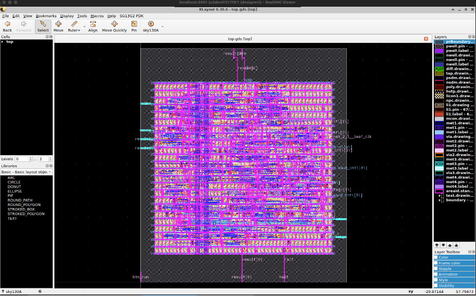
The layout shows the complete APOLLO-4G CPU with all 221 standard cells placed and fully routed across multiple metal layers. Visible on the borders: result[3], result[2], halt, btn_run, clk, baud_cnt (UART counter), and the clock tree distribution.
Tools Used
| Tool | Purpose |
|---|---|
| Python | Generate Verilog files cleanly |
| iverilog + vvp | Compile and run simulation |
| GTKWave | Waveform visualization |
| Verilator | Lint checker |
| LibreLane | Full ASIC flow — DRC/LVS/GDS |
| KLayout | GDS layout inspection |