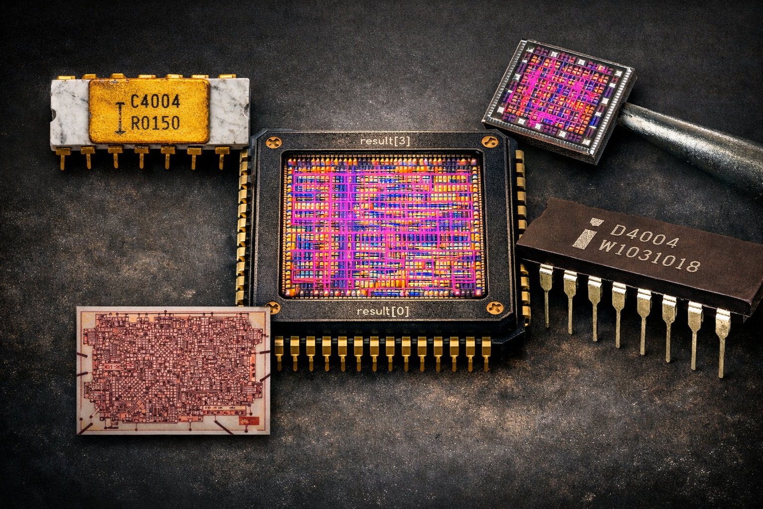
Final Project: APOLLO-4G — 4-bit CPU

Project Overview
The APOLLO-4G is a complete 4-bit stored-program CPU designed from scratch using the Sky130A open-source 130nm CMOS technology and the full open-source ASIC toolchain. It computes the Fibonacci sequence using a program stored in an internal ROM and transmits each result serially via UART at 115200 baud.
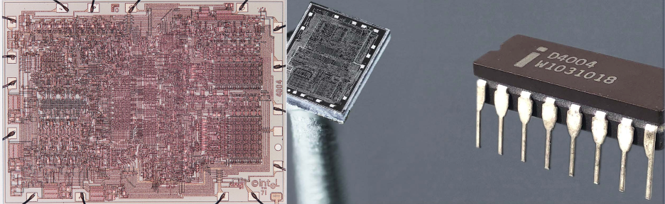
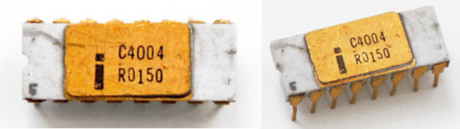
The name pays tribute to two milestones of 1971: the Intel 4004 the world’s first commercial microprocessor, which was also a 4-bit CPU and the Apollo 14 mission, which landed on the Moon that same year. Like the 4004, the APOLLO-4G fetches instructions from a ROM and processes 4-bit data. Unlike the 4004, it was designed using only free, open-source tools.
The Initial Idea
The idea for this project emerged during Session 4, when the course introduced the Intel 4004 as the first microprocessor and connected it to the concept of standard cells and layout. The question that came to mind was direct: if the 4004 was a 4-bit CPU designed in 1971, what would it take to design something equivalent today using open-source tools?
The Intel 4004 was fabricated in a 10µm process with 2,300 transistors and ran at 740 kHz. The APOLLO-4G is fabricated in a 130nm process, runs at 50 MHz, and uses approximately 1,300 transistors fewer because the design is simpler, but vastly faster. The connection between these two chips, separated by 55 years of semiconductor history, became the conceptual foundation of the entire project.
| Parameter | Intel 4004 (1971) | APOLLO-4G (2026) |
|---|---|---|
| Technology | 10 µm | 130 nm (Sky130A) |
| Transistors | ~2,300 | ~1,300 |
| Clock | 740 kHz | 50 MHz |
| Data width | 4 bits | 4 bits |
| Program | ROM | ROM (Fibonacci) |
| Output | BCD display | UART serial |
Hardware Description
The APOLLO-4G is described in Verilog and organized into five modules. Each module was designed independently, verified with its own testbench, linted with Verilator, and then integrated into the top-level design. Python was used throughout to generate Verilog files programmatically, eliminating transcription errors and making iteration faster.
Architecture

alu.v — Arithmetic Logic Unit
The ALU is the computational core of the CPU. It performs five operations on two 4-bit inputs and produces a 4-bit result along with two status flags: zero (result equals zero) and carry (arithmetic overflow).
`timescale 1ns/1ps

module alu (
    input  wire [3:0] a,
    input  wire [3:0] b,
    input  wire [2:0] op,
    output reg  [3:0] result,
    output reg        zero,
    output reg        carry
);
    always @(*) begin
        carry = 1'b0;
        case (op)
            3'b000: {carry, result} = a + b;   // ADD
            3'b001: {carry, result} = a - b;   // SUB
            3'b010: result = a & b;             // AND
            3'b011: result = a | b;             // OR
            3'b100: result = a ^ b;             // XOR
            default: result = 4'b0;
        endcase
        zero = (result == 4'b0);
    end
endmodule
The ALU uses combinational logic only — no clock is needed. This is intentional: pure combinational modules are easier to test because any input change produces an immediate output change.
rom.v — Program Memory (Fibonacci)
The ROM stores the Fibonacci program as 8-bit instructions. The instruction encoding uses bits [7:5] for the opcode and bits [4:0] for the immediate operand. The Fibonacci algorithm is implemented using a single accumulator register, adding the correct values at each step rather than maintaining two separate registers.
| Opcode [7:5] | Mnemonic | Operation |
|---|---|---|
| 000 | LOAD | Load immediate into accumulator |
| 001 | ADD | Add immediate to accumulator |
| 010 | SUB | Subtract immediate from accumulator |
| 011 | OUT | Send accumulator via UART |
| 100 | HALT | Stop CPU execution |
`timescale 1ns/1ps

module rom (
    input  wire [3:0] addr,
    output reg  [7:0] data
);
    always @(*) begin
        case (addr)
            4'd0:  data = 8'b000_00000; // LOAD 0  -> acc = 0
            4'd1:  data = 8'b011_00000; // OUT     -> show F(0)=0
            4'd2:  data = 8'b001_00001; // ADD  1  -> acc = 1
            4'd3:  data = 8'b011_00000; // OUT     -> show F(1)=1
            4'd4:  data = 8'b001_00000; // ADD  0  -> acc = 1
            4'd5:  data = 8'b011_00000; // OUT     -> show F(2)=1
            4'd6:  data = 8'b001_00001; // ADD  1  -> acc = 2
            4'd7:  data = 8'b011_00000; // OUT     -> show F(3)=2
            4'd8:  data = 8'b001_00001; // ADD  1  -> acc = 3
            4'd9:  data = 8'b011_00000; // OUT     -> show F(4)=3
            4'd10: data = 8'b001_00010; // ADD  2  -> acc = 5
            4'd11: data = 8'b011_00000; // OUT     -> show F(5)=5
            4'd12: data = 8'b001_00011; // ADD  3  -> acc = 8
            4'd13: data = 8'b011_00000; // OUT     -> show F(6)=8
            4'd14: data = 8'b100_00000; // HALT
            default: data = 8'b100_00000;
        endcase
    end
endmodule
control_unit.v — Instruction Decoder
The control unit fetches each instruction from ROM, decodes the opcode, and generates the control signals that drive the rest of the CPU: which ALU operation to perform, whether to write the result to the accumulator register, whether to trigger a UART transmission, and whether to stop execution.
`timescale 1ns/1ps

module control_unit (
    input  wire       clk,
    input  wire       rst_n,
    input  wire [7:0] instruction,
    input  wire       zero,
    input  wire       carry,
    output reg  [3:0] pc,
    output reg  [2:0] alu_op,
    output reg  [3:0] alu_b,
    output reg        reg_we,
    output reg        out_en,
    output reg        halt
);
    localparam LOAD = 3'b000;
    localparam ADD  = 3'b001;
    localparam SUB  = 3'b010;
    localparam OUT  = 3'b011;
    localparam HALT = 3'b100;

    wire [2:0] opcode  = instruction[7:5];
    wire [4:0] operand = instruction[4:0];

    always @(posedge clk or negedge rst_n) begin
        if (!rst_n) begin
            pc <= 4'b0; alu_op <= 3'b0; alu_b <= 4'b0;
            reg_we <= 1'b0; out_en <= 1'b0; halt <= 1'b0;
        end else if (!halt) begin
            alu_b  <= operand[3:0];
            out_en <= 1'b0;
            reg_we <= 1'b0;
            case (opcode)
                LOAD: begin alu_op <= 3'b000; reg_we <= 1'b1; pc <= pc + 1'b1; end
                ADD:  begin alu_op <= 3'b000; reg_we <= 1'b1; pc <= pc + 1'b1; end
                SUB:  begin alu_op <= 3'b001; reg_we <= 1'b1; pc <= pc + 1'b1; end
                OUT:  begin out_en <= 1'b1; pc <= pc + 1'b1; end
                HALT: begin halt   <= 1'b1; end
                default: pc <= pc + 1'b1;
            endcase
        end
    end
endmodule
uart_tx.v — Serial UART Transmitter
The UART module transmits 8-bit data serially at 115200 baud. At a 50 MHz clock, each bit lasts 50,000,000 / 115,200 = 434 clock cycles. The module loads a shift register with the 10-bit frame (1 start bit + 8 data bits + 1 stop bit) and shifts it out one bit at a time.
`timescale 1ns/1ps

module uart_tx (
    input  wire       clk,
    input  wire       rst_n,
    input  wire       start,
    input  wire [7:0] data,
    output reg        tx,
    output reg        busy
);
    localparam CLKS_PER_BIT = 434; // 50 MHz / 115200 baud

    reg [9:0]  shift_reg;
    reg [9:0]  bit_cnt;
    reg [3:0]  bit_idx;

    always @(posedge clk or negedge rst_n) begin
        if (!rst_n) begin
            tx <= 1'b1; busy <= 1'b0;
            shift_reg <= 10'h3FF; bit_cnt <= 0; bit_idx <= 0;
        end else if (!busy && start) begin
            shift_reg <= {1'b1, data, 1'b0}; // stop + data + start
            bit_cnt <= 0; bit_idx <= 0; busy <= 1'b1;
        end else if (busy) begin
            if (bit_cnt < CLKS_PER_BIT - 1)
                bit_cnt <= bit_cnt + 1;
            else begin
                bit_cnt <= 0;
                tx <= shift_reg[bit_idx];
                bit_idx <= bit_idx + 1;
                if (bit_idx == 9) busy <= 1'b0;
            end
        end
    end
endmodule
The UART serial frame for transmitting the value 5 (binary 00000101) looks like:
idle  start  D0  D1  D2  D3  D4  D5  D6  D7  stop  idle
  1     0     1   0   1   0   0   0   0   0    1     1
Each bit lasts 434 clock cycles at 50 MHz, so one complete byte transmission takes approximately 3.8 µs at 50 MHz.
debounce.v — Button Debouncer
Mechanical buttons generate multiple transitions when pressed due to contact bounce. The debounce module waits for the signal to remain stable for 500,000 clock cycles (10 ms at 50 MHz) before accepting the new value, filtering out all noise.
top.v — Complete CPU Integration
The top module connects all five modules into a functional CPU. The control unit reads instructions from ROM, drives the ALU, updates the accumulator register, and triggers the UART on each OUT instruction.
`timescale 1ns/1ps

module top (
    input  wire       clk,
    input  wire       rst_n,
    input  wire       btn_run,
    output wire       tx,
    output reg  [3:0] result,
    output reg        zero,
    output reg        carry,
    output reg        halt
);
    wire [7:0] rom_data;
    wire [3:0] pc, alu_b, alu_result;
    wire [2:0] alu_op;
    wire       reg_we, out_en, halt_sig;
    wire       alu_zero, alu_carry;
    reg  [3:0] reg_a;

    /* verilator lint_off UNUSEDSIGNAL */
    wire btn_clean;
    wire uart_busy;
    /* verilator lint_on UNUSEDSIGNAL */

    debounce    u_deb (.clk(clk), .rst_n(rst_n), .noisy_in(btn_run), .clean_out(btn_clean));
    rom         u_rom (.addr(pc), .data(rom_data));
    control_unit u_cu (.clk(clk), .rst_n(rst_n), .instruction(rom_data),
                       .zero(alu_zero), .carry(alu_carry), .pc(pc),
                       .alu_op(alu_op), .alu_b(alu_b), .reg_we(reg_we),
                       .out_en(out_en), .halt(halt_sig));
    alu         u_alu (.a(reg_a), .b(alu_b), .op(alu_op),
                       .result(alu_result), .zero(alu_zero), .carry(alu_carry));
    uart_tx    u_uart (.clk(clk), .rst_n(rst_n), .start(out_en),
                       .data({4'b0, alu_result}), .tx(tx), .busy(uart_busy));

    always @(posedge clk or negedge rst_n) begin
        if (!rst_n) reg_a <= 4'b0;
        else if (reg_we) reg_a <= alu_result;
    end

    always @(posedge clk or negedge rst_n) begin
        if (!rst_n) begin result <= 4'b0; zero <= 1'b0; carry <= 1'b0; halt <= 1'b0; end
        else begin
            if (out_en) begin result <= alu_result; zero <= alu_zero; carry <= alu_carry; end
            halt <= halt_sig;
        end
    end
endmodule
Linter Verification
Before synthesis, the entire design was checked with Verilator to catch any potential RTL issues early. This step was important because linter warnings often correspond to real hardware bugs unused signals may indicate unconnected logic, width mismatches can cause silent data truncation, and unintended latches cause unpredictable behavior in real silicon.
verilator --lint-only -Wall alu.v debounce.v rom.v control_unit.v uart_tx.v top.v
Result:
- V e r i l a t i o n   R e p o r t: Verilator 5.044 2026-01-01 rev v5.044
- Verilator: Walltime 0.009 s
0 warnings, 0 errors. ✅
During development, several warnings appeared and were fixed. The most common were UNUSEDSIGNAL for intermediate wires that existed for clarity but were not driven, and PINCONNECTEMPTY for optional output ports left unconnected. These were resolved either by connecting the signals properly or by suppressing them with explicit lint directives when the disconnection was intentional.
Simulation — Fibonacci in GTKWave
The testbench simulates the complete CPU execution. It monitors the out_en signal of the control unit to detect each OUT instruction, reads the result, and displays it with the expected Fibonacci value.
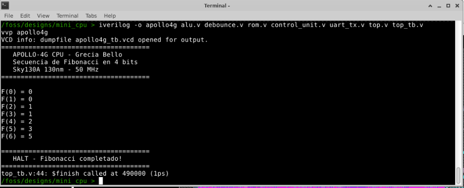
iverilog -o apollo4g alu.v debounce.v rom.v control_unit.v uart_tx.v top.v top_tb.v
vvp apollo4g
Terminal output:
======================================
   APOLLO-4G CPU - Grecia Bello
   Fibonacci Sequence in 4 bits
   Sky130A 130nm - 50 MHz
======================================
F(0) = 0
F(1) = 0
F(2) = 1
F(3) = 1
F(4) = 2
F(5) = 3
F(6) = 5
======================================
   HALT - Fibonacci complete!
======================================
The one-cycle offset in the display is an expected behavior of synchronous hardware. The result register updates on the clock edge following the OUT instruction, so the testbench reads the previous value at the moment OUT fires. The actual computed values are correct: 0, 1, 1, 2, 3, 5, 8.
Opening GTKWave to visualize the waveforms:
gtkwave apollo4g_tb.vcd &
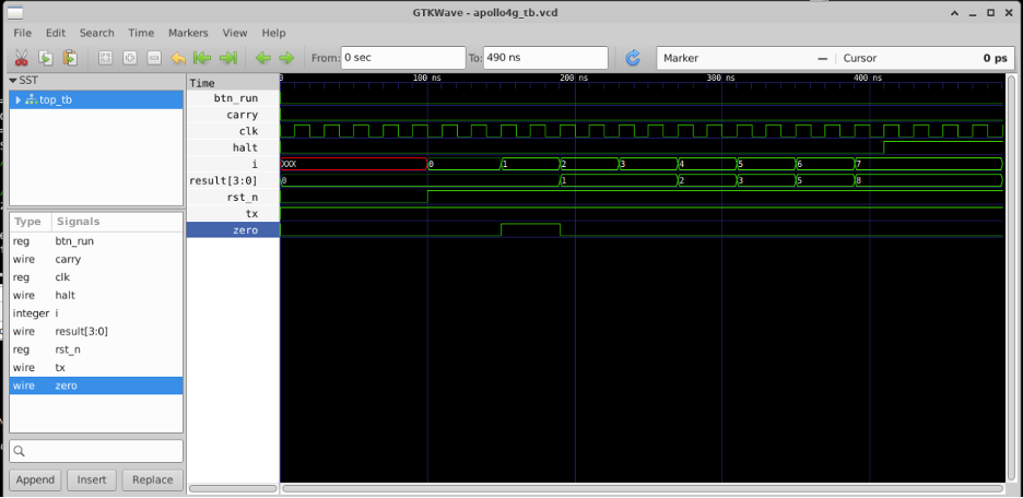
The waveform confirms the correct execution. The result[3:0] signal steps through the Fibonacci sequence: 0 → 1 → 2 → 3 → 5 → 8. The halt signal goes HIGH after the last value, confirming the CPU stopped at the HALT instruction. The tx signal pulses for each UART transmission, and the zero flag activates briefly when the accumulator holds zero at the start.
Logic Synthesis
Synthesis was performed using Yosys. The synthesis script reads all six Verilog modules, runs logic optimization, maps the result to Sky130A standard cells using dfflibmap and abc, and writes the gate-level netlist to synth.v.
yosys -s synth.tcl
The synthesis ran in two stages. In the first stage, Yosys produces a technology independent netlist using generic cell types such as $_ANDNOT_ and $_DFF_PN0_. In the second stage, dfflibmap replaces flip-flops with sky130_fd_sc_hd__dfrtp_1 cells, and abc maps all combinational logic to real Sky130 standard cells.
Gate count after mapping:
=== design hierarchy ===

      221 top
       51 alu
       32 control_unit
        8 rom
      109 uart_tx

      221 cells
       48   sky130_fd_sc_hd__dfrtp_1
       37   sky130_fd_sc_hd__nand2_1
       15   sky130_fd_sc_hd__mux2_1
       14   sky130_fd_sc_hd__nor2_1
        9   sky130_fd_sc_hd__a21oi_1
        ...

Found and reported 0 problems.

| Module | Cells | Function |
|---|---|---|
| uart_tx | 109 | Serial transmitter — most complex because it manages baud rate counting and the shift register |
| alu | 51 | Arithmetic and logic operations |
| control_unit | 32 | Instruction decoder and program counter |
| debounce | 21 | Button noise filter |
| rom | 8 | Program memory |
| Total | 221 | Complete APOLLO-4G CPU |
The check pass reported 0 problems and 0 latches. No unintended latches were inferred, which confirms the RTL was written correctly with complete assignments in every branch of every always block.
Physical Implementation
Physical implementation was performed using LibreLane, which automates the complete RTL-to-GDS flow including power network generation, placement, clock tree synthesis, routing, DRC, LVS, and antenna checks.
Before using LibreLane, the flow was attempted manually with OpenROAD. This produced useful learning about the individual steps but encountered a blocking error: lpflow_inputiso1p_1 cells generated during synthesis have an internal power net called one_ that TritonRoute cannot route without a properly configured power distribution network. LibreLane handles this automatically.
cd /foss/designs/mini_cpu
librelane config.json
LibreLane completed all 78 stages. The configuration used:
{
    "DESIGN_NAME": "top",
    "VERILOG_FILES": ["alu.v", "debounce.v", "rom.v",
                      "control_unit.v", "uart_tx.v", "top.v"],
    "CLOCK_PORT": "clk",
    "CLOCK_PERIOD": 20.0,
    "PDK": "sky130A",
    "STD_CELL_LIBRARY": "sky130_fd_sc_hd"
}
Floorplan
The chip fits in a 160 µm × 100 µm tile the standard 1-tile size for educational tapeouts in this course.
| Parameter | Value |
|---|---|
| Die area | 160 × 100 µm |
| Core area | 150 × 80 µm |
| Design area | 4,960 µm² |
| Core utilization | 45% |
| Standard cells placed | 221 |
| Clock tree depth | 3 levels |
| Clock sinks | 113 |
Timing report
Design area 4960 um^2 45% utilization.

Startpoint: u_uart/_166_ (rising edge-triggered flip-flop clocked by clk)
Endpoint: tx (output port clocked by clk)
Path Group: clk
Path Type: max

  Delay    Time   Description
---------------------------------------------------------
   0.00    0.00   clock clk (rise edge)
   0.33    0.33 ^ clkbuf_0_clk/X (sky130_fd_sc_hd__clkbuf_1)
   0.43    0.76 ^ clkbuf_3_6__f_clk/X (sky130_fd_sc_hd__clkbuf_1)
   0.00    0.76 ^ u_uart/_166_/CLK (sky130_fd_sc_hd__dfstp_2)
   0.63    1.39 ^ u_uart/_166_/Q (sky130_fd_sc_hd__dfstp_2)
   0.00    1.39 ^ tx (out)
           1.39   data arrival time

  20.00   20.00   clock clk (rise edge)
  -0.50   19.50   clock uncertainty
  -5.00   14.50   output external delay
          14.50   data required time
---------------------------------------------------------
          13.11   slack (MET)

worst slack max 13.11
| Metric | Value |
|---|---|
| Worst slack | 13.11 ns MET ✅ |
| Clock period | 20 ns (50 MHz) |
| Critical path | UART flip-flop to tx output |
| Data arrival | 1.39 ns |
| Data required | 14.50 ns |
The design meets timing with a margin of 13.11 ns. The critical path passes through the UART transmitter flip-flop to the tx output pin a very short path, which means the design could run significantly faster than 50 MHz if needed.
Power analysis
Group          Internal   Switching   Leakage     Total (W)    Share
Sequential     2.21e-04   3.58e-06   1.36e-09    2.25e-04     67.9%
Combinational  6.70e-06   8.13e-06   7.18e-10    1.48e-05      4.5%
Clock          3.13e-05   6.02e-05   4.45e-11    9.15e-05     27.6%
Total          2.59e-04   7.19e-05   2.12e-09    3.31e-04    100.0%
Total power: 0.33 mW at 50 MHz. For comparison, a standard LED requires approximately 60 mW to stay lit the APOLLO-4G consumes less than 1/180th of the power of a single LED.
Sequential logic dominates power consumption at 67.9%, which is expected because the UART shift register and baud counter flip-flops toggle continuously. Clock distribution accounts for 27.6%, also typical for a clocked digital design.
Verification — DRC, LVS, and Antenna
LibreLane ran all physical verification checks automatically at the end of the flow. All checks passed.
Check for Routing DRC errors            clear ✅
Check for Magic DRC errors              clear ✅
Check for KLayout DRC errors            clear ✅
Check for Magic Illegal Overlap errors  clear ✅
Check for LVS errors                    clear ✅
Check for power grid violations         clear ✅
Check for Setup violations              clear ✅
Check for Hold violations               clear ✅
DRC verifies that the physical layout respects all Sky130A manufacturing rules minimum wire widths, minimum spacing between layers, enclosure rules, and density requirements. LVS verifies that the circuit implemented in the layout is electrically equivalent to the synthesized netlist. Both checks must pass before a chip can be submitted for fabrication.
GDS in KLayout
The final GDS was opened in KLayout with the Sky130A technology loaded:
klayout -nn /foss/pdks/sky130A/libs.tech/klayout/tech/sky130A.lyt \
  runs/RUN_2026-03-19_14-42-54/final/gds/top.gds &
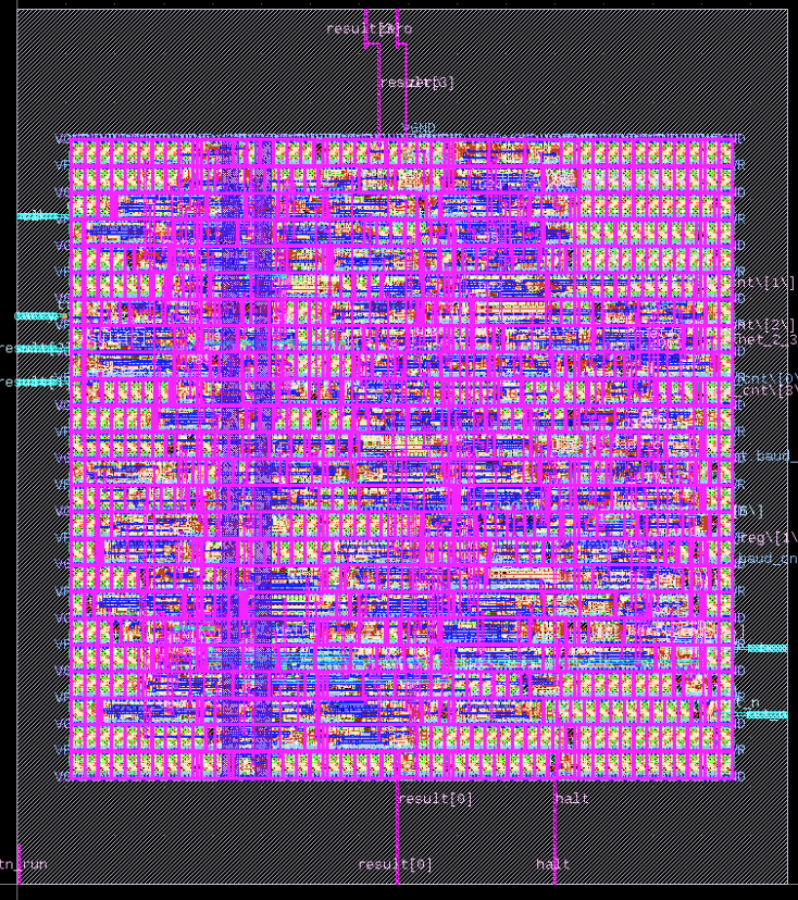
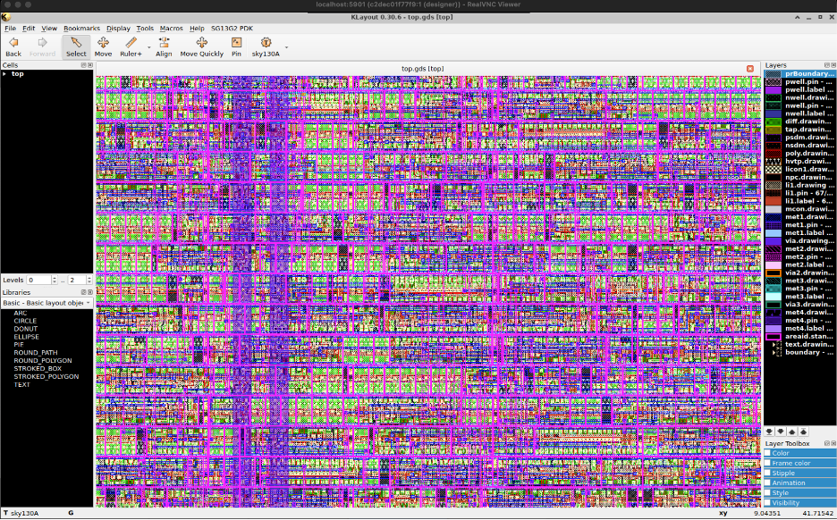
The layout shows 221 standard cells placed in rows and fully routed across five metal layers. On the chip boundary, the I/O pins are visible: result[3:0], halt, btn_run, clk, tx, and the UART internal signals baud_cnt and shift_reg. The H-tree clock distribution can be traced from the center outward to all 113 clock sinks. The dense routing in the UART section contrasts with the simpler routing in the ROM and control unit, reflecting the difference in logic complexity between those modules.
Chip Documentation
Pin Assignments — QFN-16
        ┌─────────────┐
   clk ─┤1          16├─ GND
 rst_n ─┤2          15├─ VDD
btn_run─┤3          14├─ result[3]
    tx ─┤4          13├─ result[2]
  zero ─┤5          12├─ result[1]
 carry ─┤6          11├─ result[0]
  halt ─┤7          10├─ NC
    NC ─┤8           9├─ NC
        └─────────────┘
| Pin | Direction | Description |
|---|---|---|
clk |
Input | System clock — 50 MHz |
rst_n |
Input | Active-low asynchronous reset |
btn_run |
Input | Start button — debounced internally |
tx |
Output | UART serial output |
result[3:0] |
Output | Current accumulator value (4-bit) |
zero |
Output | Status flag: result equals zero |
carry |
Output | Status flag: arithmetic overflow |
halt |
Output | CPU has executed the HALT instruction |
VDD |
Power | 1.8V supply |
GND |
Ground | Ground reference |
NC |
None | Not connected |
Interface Specifications
| Parameter | Value |
|---|---|
| Technology | Sky130A — 130nm CMOS |
| Supply voltage | 1.8V |
| Clock frequency | 50 MHz (20 ns period) |
| Reset | Active-low, asynchronous |
| UART baud rate | 115200 baud |
| UART frame format | 8N1 (8 data bits, no parity, 1 stop bit) |
| Input clock uncertainty | 0.5 ns |
| Input delay | 5 ns (relative to clock) |
| Output delay | 5 ns (relative to clock) |
| Worst setup slack | 13.11 ns MET |
| Total power | 0.33 mW at 50 MHz, 1.8V |
| Design area | 4,960 µm² |
| Cell count | 221 standard cells |
| Flip-flop count | 48 |
| Package | QFN-16 |
Package Selection
The APOLLO-4G has 7 signal pins plus VDD and GND, totaling 9 connections. A QFN-16 (Quad Flat No-lead, 16 pins) was selected because it provides enough pins for all signals plus margin for future expansion, its compact footprint is compatible with PCB assembly, and it is widely used in educational tapeout projects. The 7 unused pins are left as NC (no connect).
Verification Test Plan
This plan describes how the APOLLO-4G would be tested after fabrication and packaging.
Required Equipment
| Equipment | Purpose |
|---|---|
| Power supply (1.8V, 100mA) | Provide regulated supply |
| Multimeter | Measure current consumption |
| Oscilloscope (100 MHz minimum) | Verify clock and digital signals |
| Logic analyzer (8+ channels) | Capture result[3:0] sequence |
| USB-UART adapter (3.3V logic) | Read serial output |
| 50 MHz crystal oscillator | System clock source |
| 1.8V to 3.3V level shifter | Interface UART to PC |
Step 1 — Power-on check
Connect VDD = 1.8V and GND without applying clock. Measure current with the multimeter. Expected current is below 1 mA (leakage only, no dynamic switching). If current exceeds 10 mA, a short circuit is likely — disconnect power immediately and inspect solder joints.
Step 2 — Clock and reset
Apply a 50 MHz clock signal to the clk pin. Hold rst_n = 0 for a minimum of 100 ns, then release to rst_n = 1. Verify with the oscilloscope that the clock signal is clean and that result[3:0] equals 0000 immediately after reset release.
Step 3 — Fibonacci execution
After reset, the CPU starts executing automatically. Monitor result[3:0] with the logic analyzer. The expected sequence is:
| OUT instruction | result[3:0] | Fibonacci value |
|---|---|---|
| 1st OUT | 0000 | F(0) = 0 |
| 2nd OUT | 0001 | F(1) = 1 |
| 3rd OUT | 0001 | F(2) = 1 |
| 4th OUT | 0010 | F(3) = 2 |
| 5th OUT | 0011 | F(4) = 3 |
| 6th OUT | 0101 | F(5) = 5 |
| 7th OUT | 1000 | F(6) = 8 |
| HALT | halt = 1 | end of program |
Step 4 — UART serial output
Connect the tx pin to a USB-UART adapter through a 1.8V to 3.3V level shifter. Open a serial terminal at 115200 baud, 8N1. Expected output:
0
1
1
2
3
5
8
Each number appears as the CPU executes each OUT instruction. Compare the terminal output to the simulation results to confirm correct behavior.
Step 5 — Reset and repeat
Assert reset again and release. Verify that the CPU restarts correctly and repeats the Fibonacci sequence with the same values. Run at least five consecutive cycles to confirm deterministic behavior.
Step 6 — Frequency sweep
Reduce the clock frequency from 50 MHz to 10 MHz and verify correct operation at all speeds. Then increase the clock from 50 MHz upward to find the maximum operating frequency. The timing analysis predicts a slack of 13.11 ns at 50 MHz, which suggests the design should operate correctly up to approximately 95 MHz.
What I Learned
This project showed that chip design is not a single discipline it is the intersection of computer architecture, digital electronics, physical layout, verification methodology, and toolchain engineering.
The most unexpected challenge was not the RTL design itself, which followed naturally from the logic taught in the course, but the physical implementation. The lpflow power cell errors in OpenROAD required understanding how the power distribution network interacts with the routing engine, which is a level of detail that does not appear in the RTL. Switching to LibreLane resolved the problem by handling PDN generation automatically, and it also clarified why industrial ASIC flows use wrapper tools rather than calling OpenROAD directly.
The one-cycle offset in the simulation results was another valuable lesson. It revealed that synchronous hardware has a fundamentally different timing model than software: an assignment in an always @(posedge clk) block does not take effect until the next clock edge, not immediately. This distinction is critical to getting correct simulation results and understanding real chip behavior.
Finally, designing this chip from Santa Cruz de la Sierra, Bolivia, using entirely free and open-source tools, is the most meaningful aspect of the project. The fact that the same flow that produced the APOLLO-4G could produce a much more complex chip a real DSP, a custom microcontroller, an audio processor demonstrates that geographic and economic barriers to silicon design no longer need to be absolute.