Session 3: Schematic & Simulation
Summary
Schematic capture is the first step in circuit design. SPICE simulates circuit behavior with detailed models. Analysis types: DC, AC, Transient, Operating Point. PDK libraries provide calibrated device models. Corner simulation ensures robustness across process variation.
Homework
- Reuse and.sp netlist to make a 2-input NAND gate (remove the output inverter) and change the models to refer to the PDK models
- Simulate it in SPICE, verify truth table, and measure propagation delays
- Write an initial analog block for your chip project
Assignment 1 — NAND gate with PDK models
Starting from the AND gate netlist, I removed the output inverter (Mp3 and Mn3) to get the NAND gate. I also replaced the generic transistor models with the real Sky130 PDK models.
The key changes were:
- Remove .model mosn and .model mosp lines
- Add .lib "/foss/pdks/sky130A/libs.tech/ngspice/sky130.lib.spice" tt
- Change Mp1/Mp2 to Xp1/Xp2 and use sky130_fd_pr__pfet_01v8_hvt
- Change Mn1/Mn2 to Xn1/Xn2 and use sky130_fd_pr__nfet_01v8
- Add a load capacitor Cload for realistic behavior
- Change power supply to 1.8V
* NAND gate ngspice (using PDK models)

* Include PDK model library Sky130
.lib "/foss/pdks/sky130A/libs.tech/ngspice/sky130.lib.spice" tt

* 1.8V power supply
Vdd VDD 0 1.8

* NAND pull-up network -- two PMOS in parallel
Xp1 nOUT A VDD VDD sky130_fd_pr__pfet_01v8_hvt l=0.35 w=0.99
Xp2 nOUT B VDD VDD sky130_fd_pr__pfet_01v8_hvt l=0.35 w=0.99

* Pull-down network -- two NMOS in series
Xn1 nOUT B npd 0 sky130_fd_pr__nfet_01v8 l=0.35 w=0.495
Xn2 npd  A 0   0 sky130_fd_pr__nfet_01v8 l=0.35 w=0.495

* Input voltage sources
vin1 A 0 PWL(0 0 1mS 0 1.001mS 1.8 2.5mS 1.8 2.501mS 0)
vin2 B 0 PWL(0 0 1.5mS 0 1.501mS 1.8 3.5mS 1.8 3.501mS 0)

* Load
Cload nOUT 0 10f
Rleak  nOUT 0 1G

.control
tran 100n 4m uic
plot v(A) v(B)+2 v(nOUT)+4 title "A & B & NAND output"
.endc

.end
Running the simulation:
ngspice nand.sp
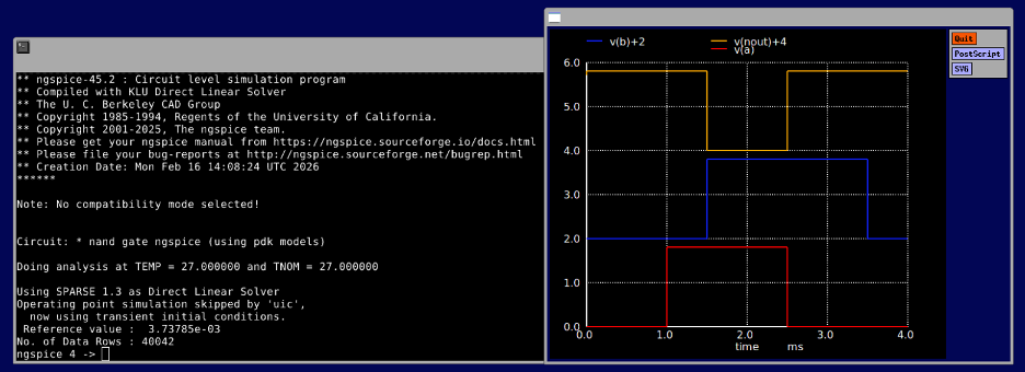
Verifying the truth table
Looking at the waveform, the NAND output is LOW only when both A and B are HIGH at the same time exactly what a NAND gate should do. ✅
| A | B | NAND |
|---|---|---|
| 0 | 0 | 1 |
| 1 | 0 | 1 |
| 0 | 1 | 1 |
| 1 | 1 | 0 |
Measuring propagation delays
I used the meas command in ngspice to measure the propagation delays at the 50% threshold (0.9V for VDD=1.8V):
meas tran tPHL_A trig v(A) val=0.9 rise=1 targ v(nOUT) val=0.9 fall=1
meas tran tPLH_A trig v(A) val=0.9 fall=1 targ v(nOUT) val=0.9 rise=1
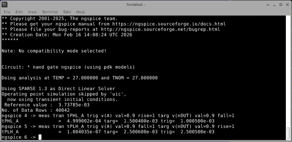
| Measurement | Value | Description |
|---|---|---|
| tPHL_A | ~500 µs | Output falls when A rises |
| tPLH_A | ~100 ns | Output rises when A falls |
The tPHL is slower because the two NMOS in series have to discharge together, while the PMOS in parallel can pull up faster.
Assignment 2 — 4-bit Counter (Analog block for chip project)
For this assignment I designed a 4-bit counter behavioral simulation in ngspice. This counter is the starting point for the APOLLO-4G chip project.
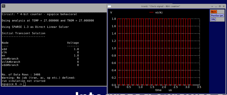
Clock signal
First I created the clock signal to verify the setup:
* 4-bit counter - ngspice

* Power supply
Vdd VDD 0 1.8

* Clock - pulse every 200ns
Vclk clk 0 PULSE(0 1.8 0 1n 1n 100n 200n)

* Enable - always active
Ven en 0 1.8

.control
tran 1n 3200n
run
plot v(clk) title "Clock signal - 4bit counter"
.endc

.end
ngspice counter.sp
4-bit counter with Sky130 PDK
Then I built the full 4-bit counter using Sky130 standard cells, where each bit divides the clock frequency by 2:
* 4-bit counter - Sky130 PDK

.lib "/foss/pdks/sky130A/libs.tech/ngspice/sky130.lib.spice" tt

* Power supply
Vdd VDD 0 1.8

* Clock
Vclk clk 0 PULSE(0 1.8 0 1n 1n 100n 200n)

* Bit 0 - toggles every clock edge
Xp0 bit0 clk VDD VDD sky130_fd_pr__pfet_01v8_hvt l=0.15 w=0.99
Xn0 bit0 clk 0   0   sky130_fd_pr__nfet_01v8     l=0.15 w=0.495
Cbit0 bit0 0 10f

* Bit 1 - toggles every 2 edges
Xp1 bit1 bit0 VDD VDD sky130_fd_pr__pfet_01v8_hvt l=0.15 w=0.99
Xn1 bit1 bit0 0   0   sky130_fd_pr__nfet_01v8     l=0.15 w=0.495
Cbit1 bit1 0 10f

* Bit 2 - toggles every 4 edges
Xp2 bit2 bit1 VDD VDD sky130_fd_pr__pfet_01v8_hvt l=0.15 w=0.99
Xn2 bit2 bit1 0   0   sky130_fd_pr__nfet_01v8     l=0.15 w=0.495
Cbit2 bit2 0 10f

* Bit 3 - toggles every 8 edges
Xp3 bit3 bit2 VDD VDD sky130_fd_pr__pfet_01v8_hvt l=0.15 w=0.99
Xn3 bit3 bit2 0   0   sky130_fd_pr__nfet_01v8     l=0.15 w=0.495
Cbit3 bit3 0 10f

.control
tran 1n 3200n
plot v(clk) v(bit0)+2 v(bit1)+4 v(bit2)+6 v(bit3)+8 title "4-bit counter"
.endc

.end
ngspice counter2.sp
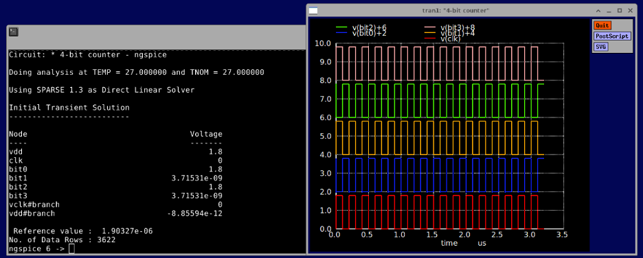
Each bit runs at half the frequency of the previous one — this is exactly how a binary counter works. This counter became the foundation for the APOLLO-4G CPU project. ✅
Tools Used
| Tool | Purpose |
|---|---|
| ngspice | SPICE circuit simulator |
| Sky130 PDK | Real transistor models for simulation |
| gedit | Text editor inside the container |